To access tsmc 0.18um pdk, mosis requires all the users to sign a Non-Disclosure Agreement (NDA). Please print a copy of the MOSIS NDA form, sign and submit to Prof. Moon to be added to the pdk user list.
This example will help you to create a layout for the inverter you designed
in the first example. It will go over the Virtuoso layout tool and how to layout mosfets, resistors, and
capacitors in our process. There are many considerations to take into account
when deciding how to do a layout. This is NOT an example on layout techniques,
but more of a generalized example to help get you farmiliar with Virtuoso and
laying-out some basic components.
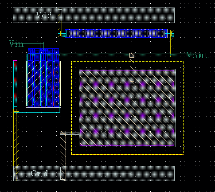
The following picture shows a layout for the inverting amplifier, ready for
extracting. The next section explains how to make each of the separate components
in Virtuoso.
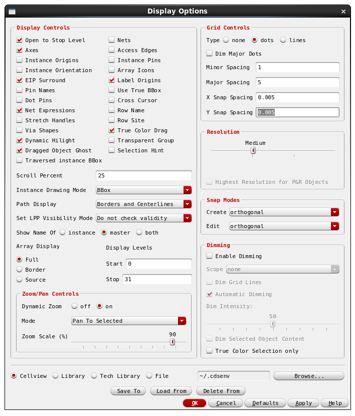
Make sure that the grid size for the layout is set to 0.005um. This is a really important step. Violating the minimum grid size can result in off-grid errors in the later stages.
To set the grid size, choose
Options->Display
Set X snap spacing and Y snap spacing to 0.005
| Creating shapes | Create->Rectangle [r] Create->Path [p] |
| Editing shapes | Edit->Move [m] Edit->Stretch [s] Edit->Copy [c] Edit->Delete [del] Edit->Properties [q] Edit->Undo [u] Edit->Redo [U] |
| Measuring distances | Misc->Ruler [k] Misc->Clear Rulers [K] |
| Window commands | Zoom In [z] Zoom In by 2 [^z] Zoom Out By 2 [Z] Fit All [f] Redraw [^r] |
Other commands | Gravity On/Off[g] Display levels (0-20) [F] Display levels (0-0) [^f] |
For this inverter we will need to layout an nmos transistor, a resistor, and a capacitor. The following sections will describe how to access the layout of these components from the pdk and how to access the terminals for routing. SOme of these steps are very similar to the schematic example.
Create->Instance
In the Add Instance window Click Browse to open Component Browser.
Make sure the Library in the Component Browser is set to tsmc18 and enable Show Categories to sort the components in the pdk library.
In the Component Browser window,
For mosfet, choose
Category: Mosfet_4T
Cell: nmos2v
View: layout
then place it.
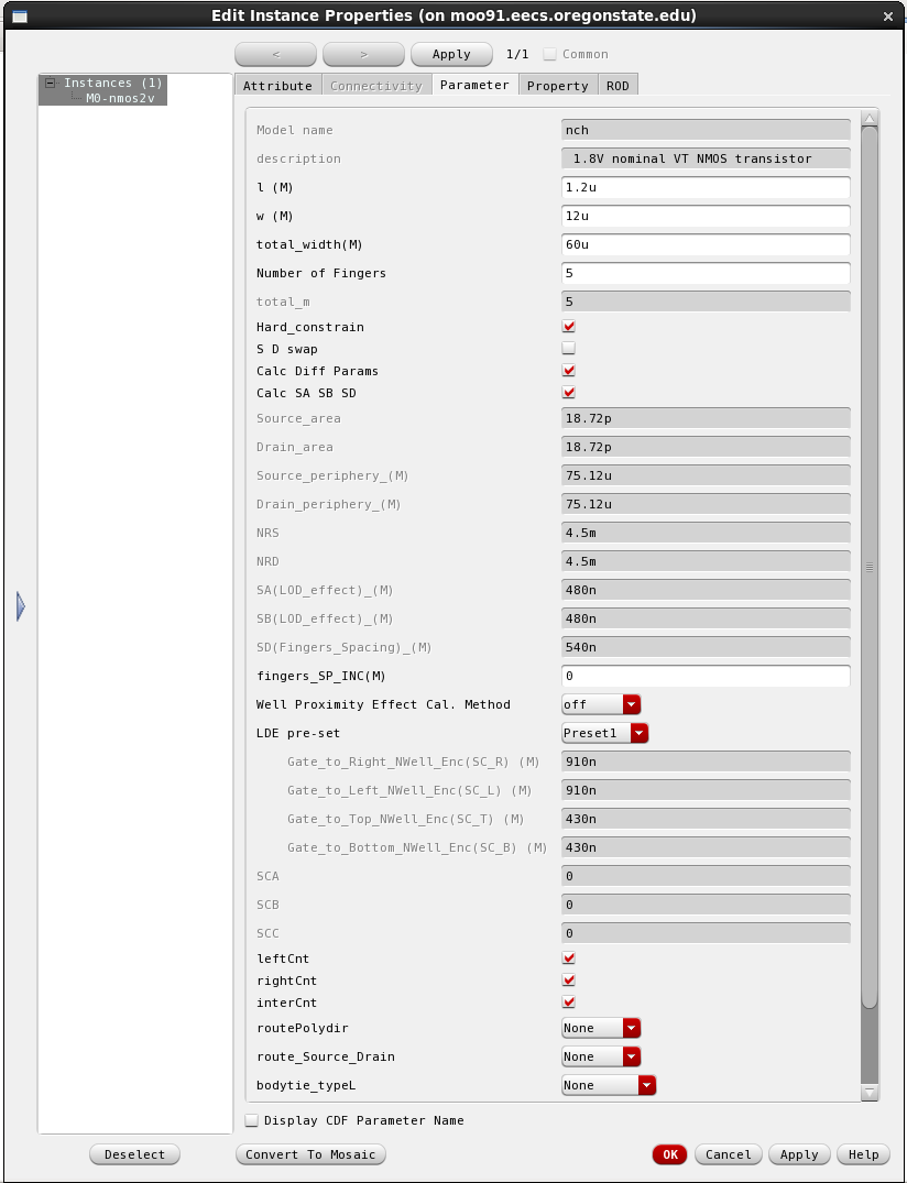
When making MOSFETs you can create a single transistor, or use fingers or multipliers to create multiple transistors at once. Fingers makes transistors which are connected in series, multipliers create transistors which are connected in parallel. For our layout example we will be using fingers to make multiple transistors which will be equivalent to one really wide transistor. However, if transistors have to be matched, multipliers are preferred.
Clicking SHIFT-F will show all levels and allow you to see inside the cell you just placed (CNTRL-F will change back to just showing the top level).
Now we need to connect together the drains, gates, and sources and place some bulk connections.
Repeat this process using metal1 to connect every other drain/source
connection together across the top.
Do the same thing for the opposite every other drain/source along the bottom.
Your finished transistor should look similar to the following:
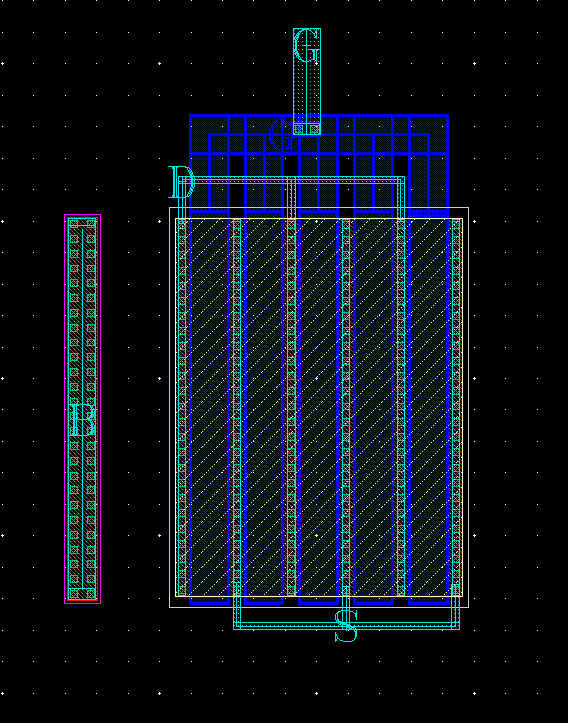
Lastly we need to create some bulk connections. We will create these across the left side of the transistor block.
Create->Instance
When placing instances you can place multiple instances in a matrix type formation by specifying the number of rows and columns to place. We will now use this to place a column of ptaps along the side of the transistor block.
We now have a transistor with single gate, drain, source, and bulk connections.
Make sure to do DRC before continuing on to make sure everything was placed
correctly.
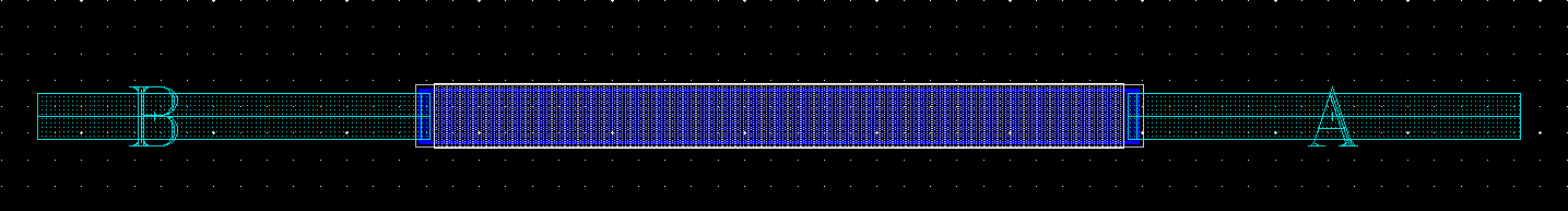
Select the resistor. Edit the segment width and segment length parameters to set a resistance of 4k Ohms.
The resistance value is given by R = sheet_resistance*(segment_length/segment_width). For rnhpoly, the sheet resistance is 295.3 ohms/square.
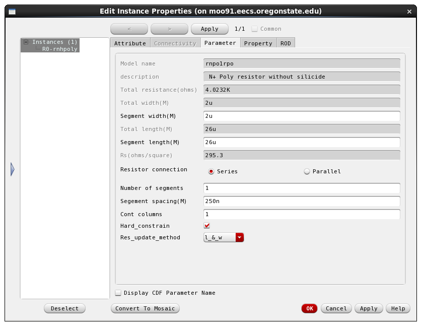
The end terminals are accesibile with Metal1. The completed resistor layout should look like the figure below.
We now have a resistor with metal1 connections on each side. Once again, make sure to do DRC before continuing on.
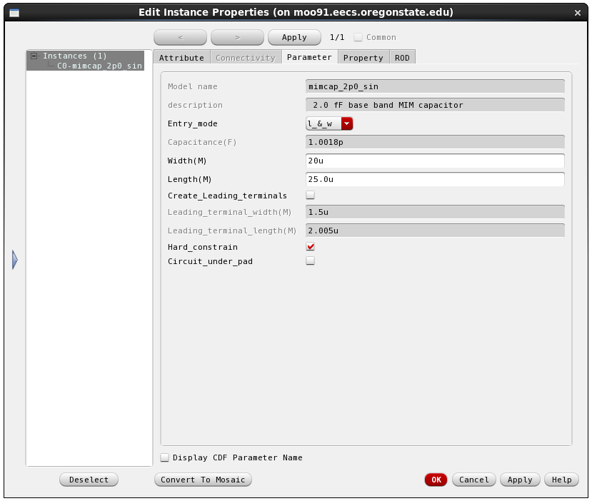
Select the capacitor. Edit the Width and Length properties to set a capacitance of 1pF.
The capacitance value is given by C = Capacitance_per_unit_area*(length*width). For mimcap_2p0_sin, the capacitance per unit area is 2fF/um2.
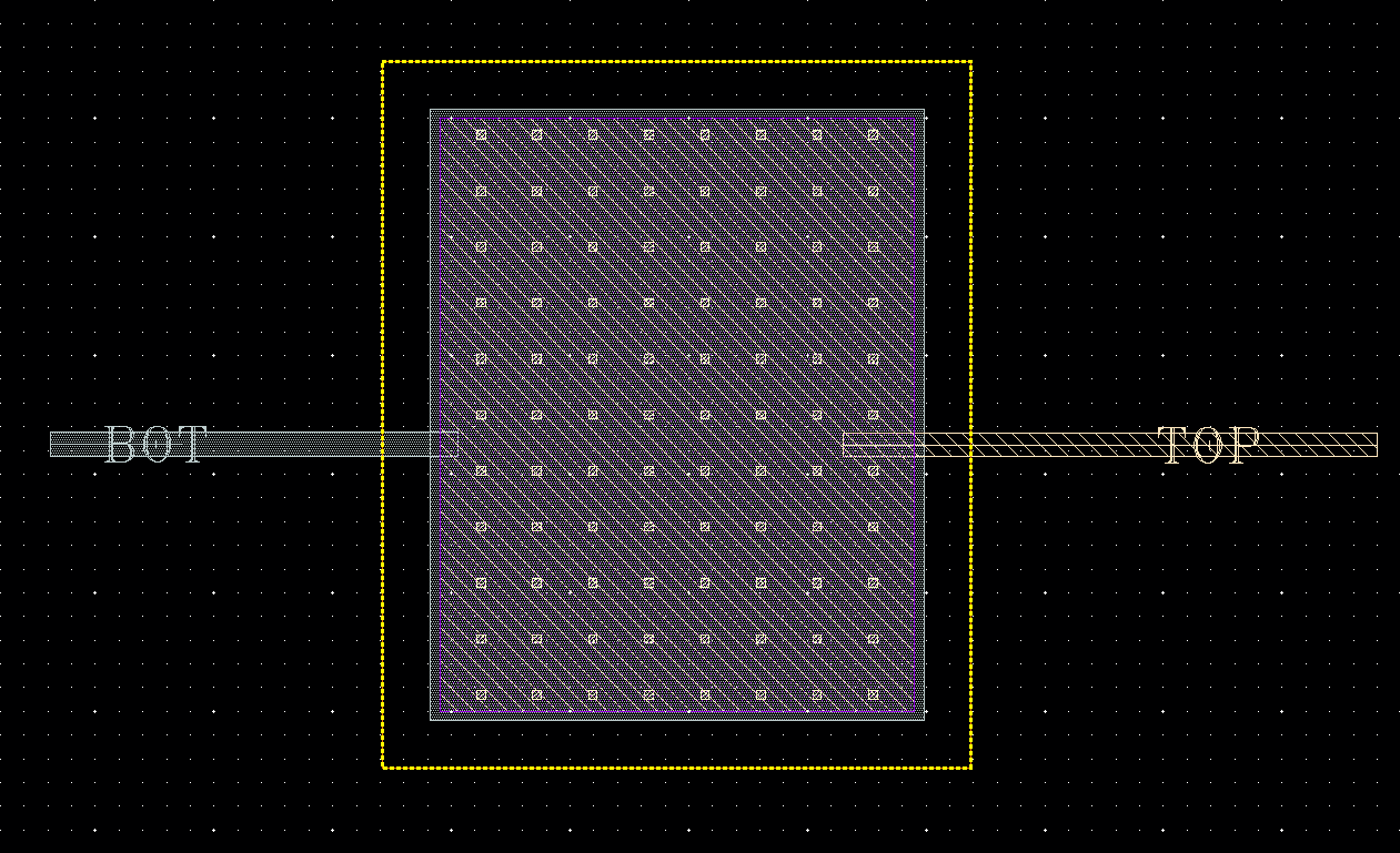
The top plate terminal is accessible with Metal6 and the bottom terminal is accessible with Metal5. The completed mimcap layout should look like the figure shown below.
Now you have a capacitor with two terminals
. Remember, make sure to do DRC
again to be sure you aren't violating any rules.
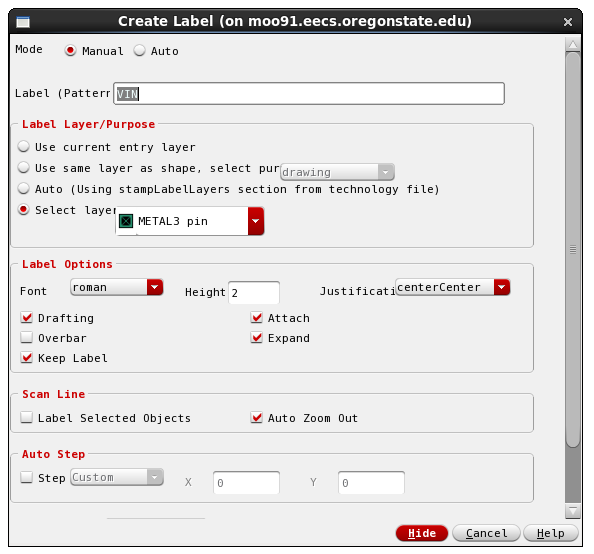
After routing all your connections for the inverter (don't forget to DRC often), you simply need to add pins for VIN, VOUT, VDD and GND.
Create->Label
After doing this for all the nodes your layout is complete!