MOSIS NDA
This is an important step to obtain access to tsmc 0.18um pdk for the class
To access tsmc 0.18um pdk, mosis requires all the users to sign a Non-Disclosure Agreement (NDA).
Please print a copy of the MOSIS NDA
form, sign and submit to Prof. Moon to be added to the pdk user list.
LAYOUT AND VERIFICATION
Design Rule Checking (DRC)
At any time during your design, you can verify if any dimensions are being
violated.
In the layout window, select:
Calibre->Run nmDRC
Calibre Interactive window opens. In the Rules tab, update the "DRC Rules File" and "DRC Run Directory" fields as
DRC Rules File: /nfs/stak/users/moon/ece423/pdk/tsmc018/Calibre/drc/calibre.drc
DRC Run Directory: ./run_drc
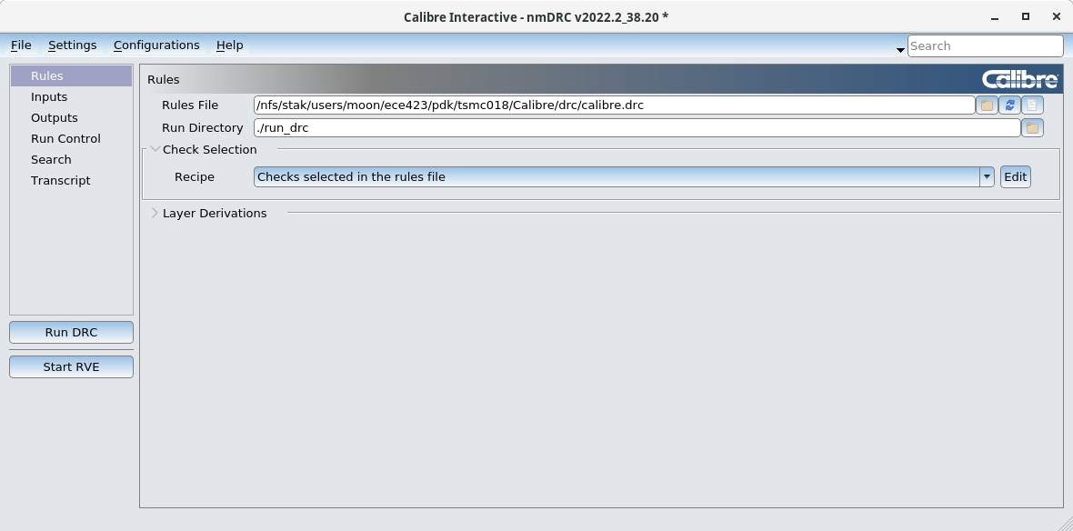
Figure 1: DRC rules and Run Directory.
In the Inputs tab, update the "DRC Rules File" and "DRC Run Directory" fields as
Run : DRC(Flat)
File: inverter.calibre.db
Top Cell: inverter (or whatever is the cellview name)
Check "Export from layout viewer" to automatically acquire layout database into calibre.
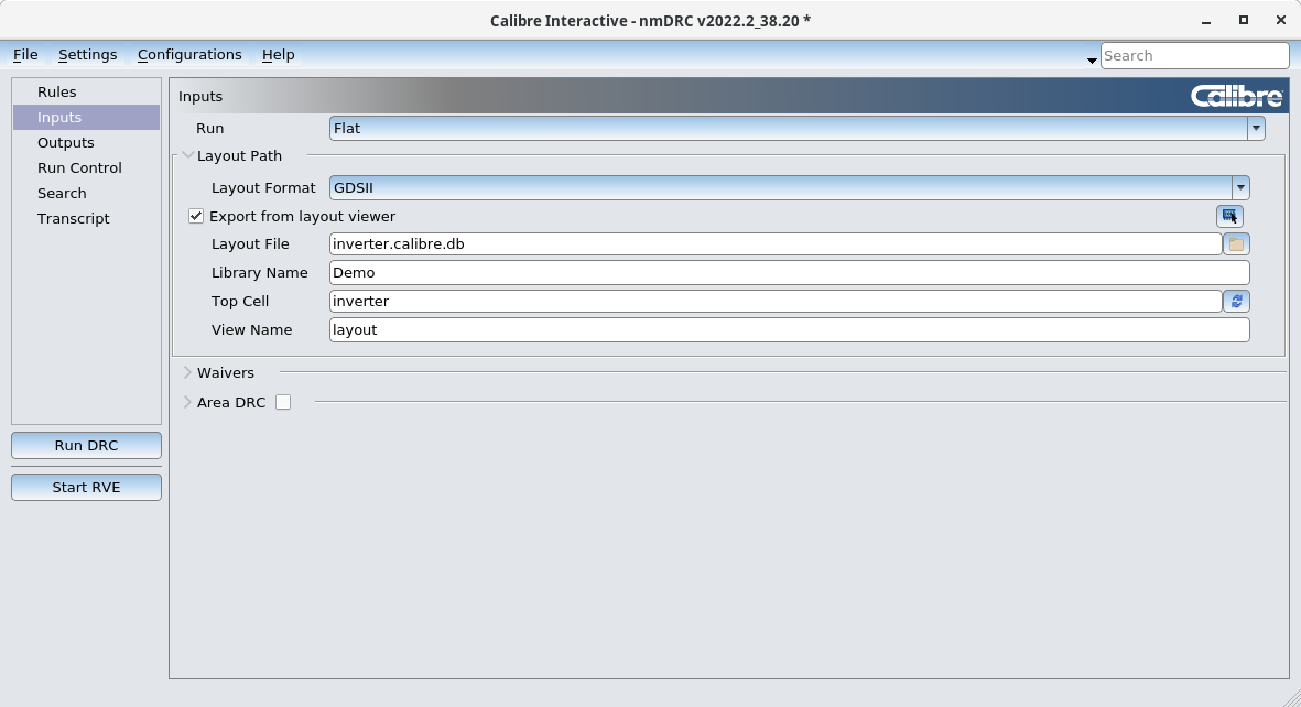
Figure 2: DRC Inputs.
Click "Run DRC" tab to start DRC run. Calibre RVE opens after the run is complete.
If DRC rules are violated in the layout, the errors are displayed in the left corner. A discreption of the error is displayed in the bottom left corner of the RVE window. For example, in the figure below, minimum space of Metal1 is violated.
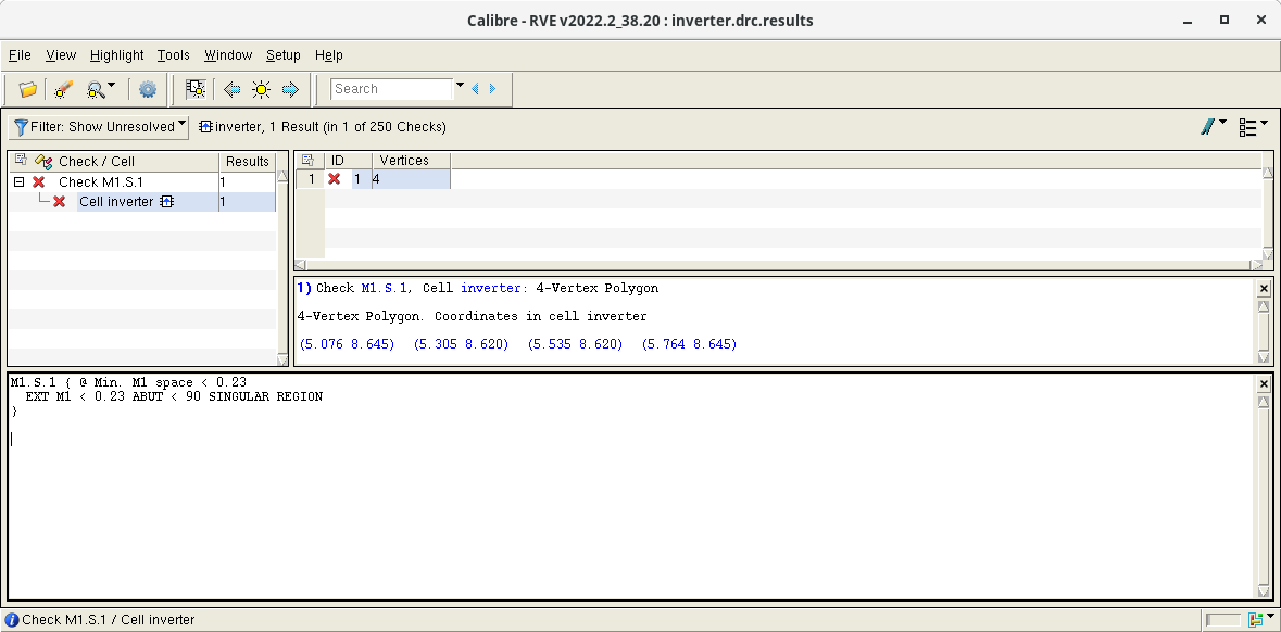
Figure 3: Calibre RVE showing DRC failure.
Update the layout to fix the DRC errors. Click "Run DRC" tab to rerun DRC. If the layout is DRC clean Calibre RVE dispalys a green checkmark on the left corner.
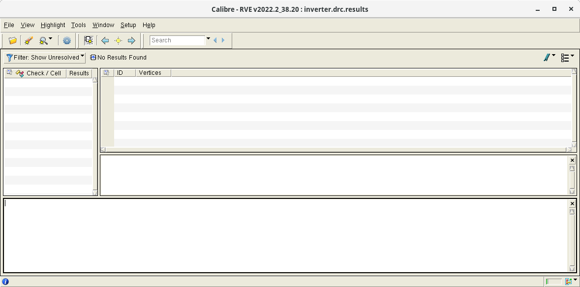
Figure 4: Calibre RVE showing DRC is clean.
Layout Versus Schematic (LVS)
The LVS tool is used to compare the layout with the schematic, identifying any circuit related differences that might exist between these two views. It reports about circuit nodes and device sizes.
In the layout window, select:
Calibre->Run nmLVS
Calibre Interactive window opens. In the Rules tab, update the "LVS Rules File" and "LVS Run Directory" fields as
pexLVS Rules File: /nfs/stak/users/moon/ece423/pdk/tsmc018/Calibre/lvs/calibre.lvs
LVS Run Directory: ./run_lvs
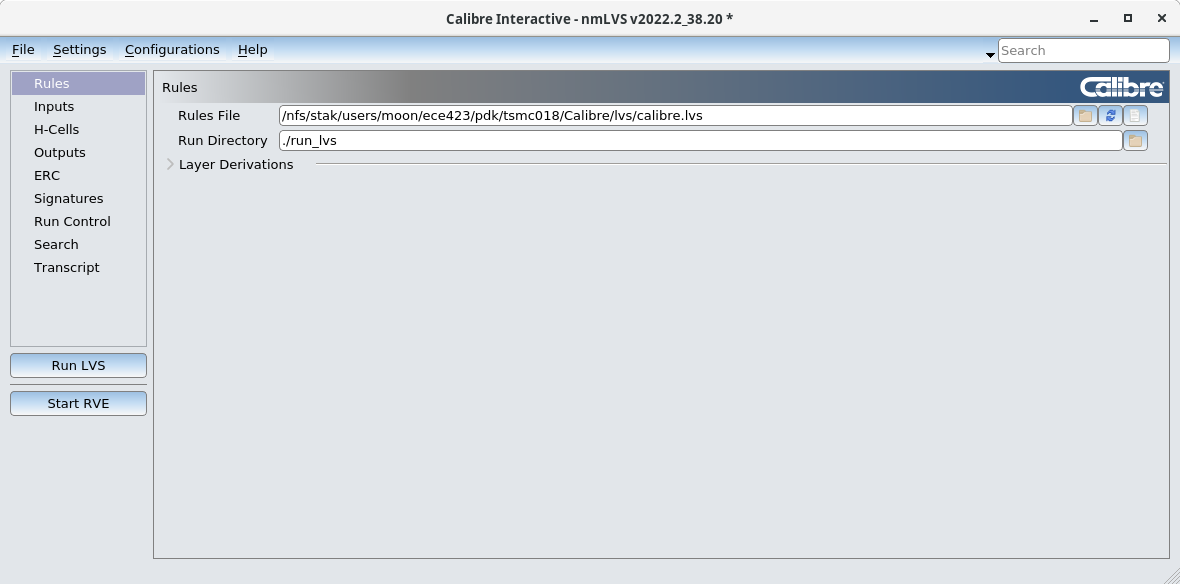
Figure 5: LVS rules and Run Directory.
In the Inputs tab, update the Layout fields as
Run: Flat
File: inverter.calibre.db
Format: GDSII
Top Cell: inverter (or whatever the cellview name is)
Library: TEST (or whatever the library name is)
View: layout
Check "Export from layout viewer" to automatically acquire layout database into calibre.
In the Inputs tab, update the Source fields as
File: inverter.src.net
Format: Spice
Top Cell: inverter (or whatever the cellview name is)
Library: TEST (or whatever the library name is)
View: schematic
Check "Export from schematic viewer" to automatically acquire schematic database into calibre.
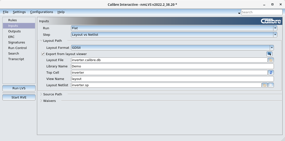
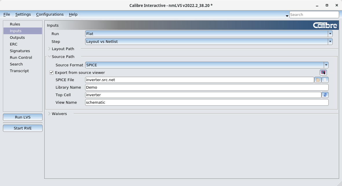
Figure 6: LVS Inputs.
To view LVS options, click Settings -> Show Pages -> Options in the calibre menu.
In the Options tab, update the Power and Ground nets
Power nets: VDD (or whatever name you set for supply pin)
Ground nets: GND (or whatever name you set for ground pin)
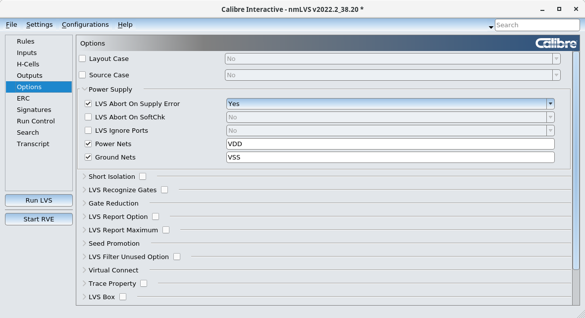
Figure 7: LVS Options.
Click "Run LVS" tab to start LVS run. Calibre RVE opens after the run is complete.
If there is a mismatch in the layout and the schematic, the errors are displayed in the RVE. Typically three types of errors can occur. Incorrect nets, Incorrect ports and Incorrect instances. Incorrect nets and ports correspond to missing connections or mismatch in the name or case of the pin or label. Incorrect instances correspond to mismatch in device dimensions between schematic and layout.
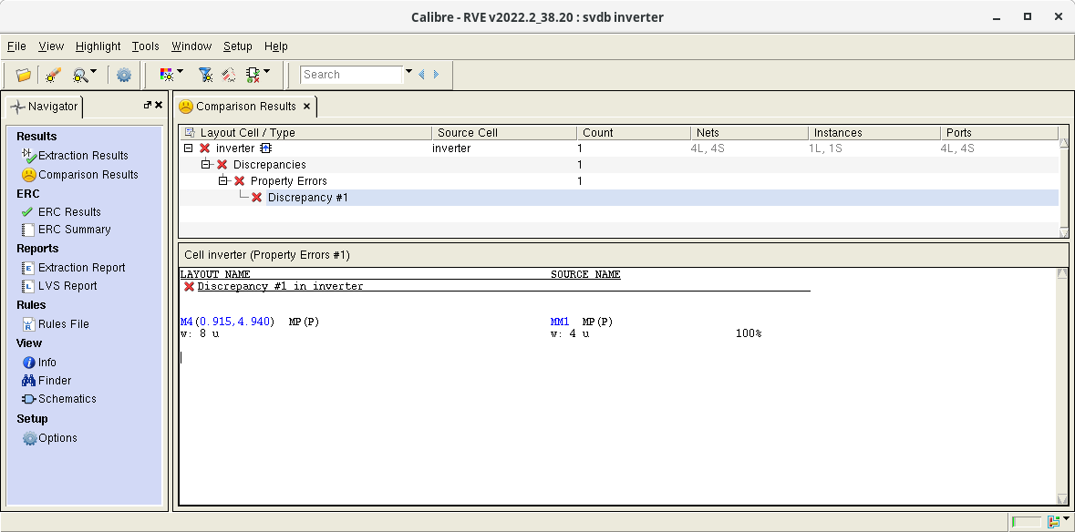
Figure 8: Calibre RVE showing LVS failure.
Update the layout to fix the LVS errors. Click "Run LVS" tab to rerun LVS. If the layout is LVS clean, Calibre RVE dispalys a green smiley face.
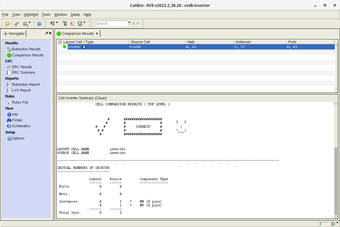
Figure 9: Calibre RVE showing LVS is clean.
Note that unlike DRC,
understanding LVS errors is not a straightforward procedure, but more of a debugging process.
Parasitic Extraction (PEX)
The PEX tool is used to extract the parasitic capacitors and resistors that result from routing in the layout.
In the layout window, select:
Calibre->Run PEX
Calibre Interactive window opens. In the Rules tab, update the "PEX Rules File" and "PEX Run Directory" fields as
PEX Rules File: /nfs/stak/users/moon/ece423/pdk/tsmc018/Calibre/rcx/calibre.rcx
PEX Run Directory: ./run_pex
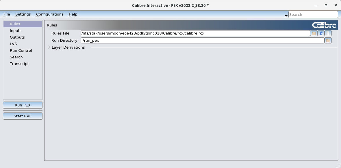
Figure 10: PEX rules and Run Directory.
In the Inputs tab, update the Layout fields as
File: inverter.calibre.db
Format: GDSII
Top Cell: inverter (or whatever the cellview name is)
Library: TEST (or whatever the library name is)
View: layout
Check "Export from layout viewer" to automatically acquire layout database into calibre.
In the Inputs tab, update the Source fields as
File: inverter.src.net
Format: Spice
Top Cell: inverter (or whatever the cellview name is)
Library: TEST (or whatever the library name is)
View: schematic
Check "Export from schematic viewer" to automatically acquire schematic database into calibre.
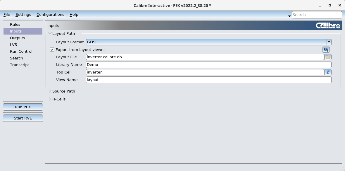
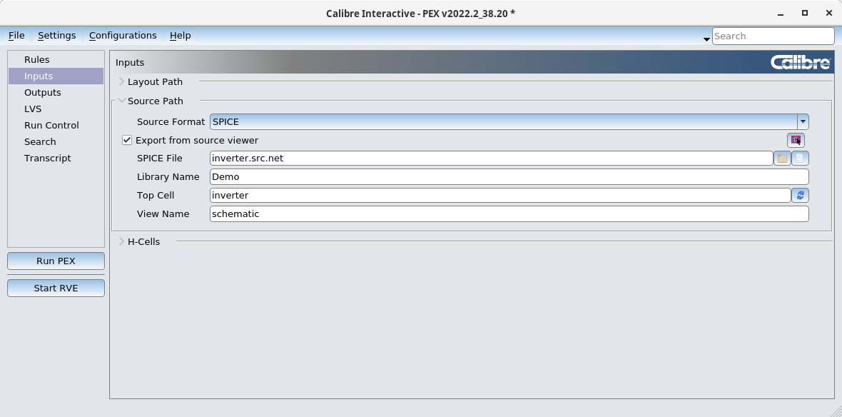
Figure 11: PEX Inputs.
In the Outputs tab, update the fields as
Extraction Mode: xRC
Extraction Type: Transistor Level, C+CC
Netlist Path: inverter.pex.netlist
Netlist Format: Calibreview
Use Names From: Schematic Only
Ground: GND (or whatever name you set for ground pin)
The extraction type can be changed to R only, R+C+CC or no R/C depending on what the designer would like to extract from the drawn layout. no R/C extraction is typicaly used to check device extraction, ignoring parasitics. This is helpful to ensure there are no connectivity issues or to ensure for example the extracted transistor parameters match closely with the schematic.
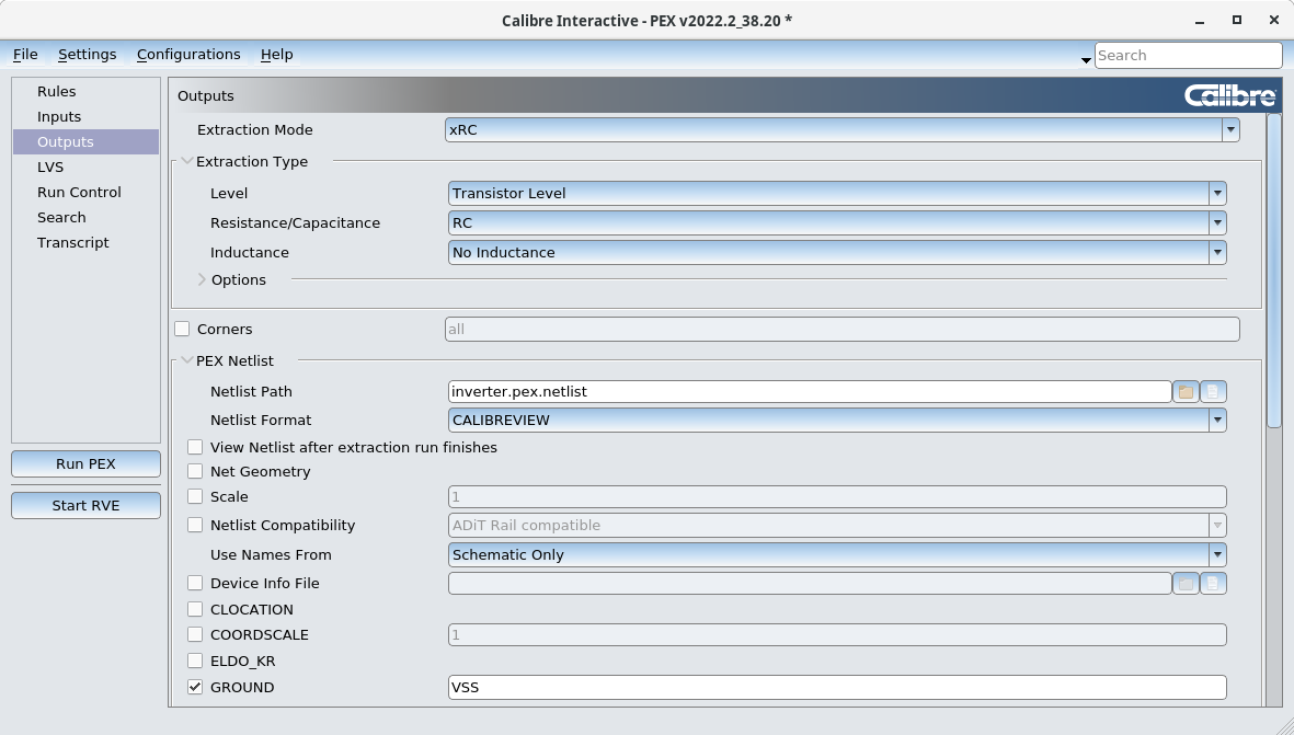
Figure 12: PEX Outputs.
In the LVS tab, update the fields as
Power nets: VDD (or whatever name you set for supply pin)
Ground nets: GND (or whatever name you set for ground pin)
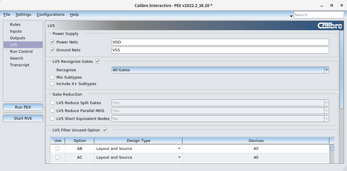
Figure 13: LVS Options.
To view PEX options, click Settings -> Show Pages -> Options in the calibre menu.
In the Options tab, update the extraction setup, such as resistance or capacitance reduction. Leave all fields as default for the class project.
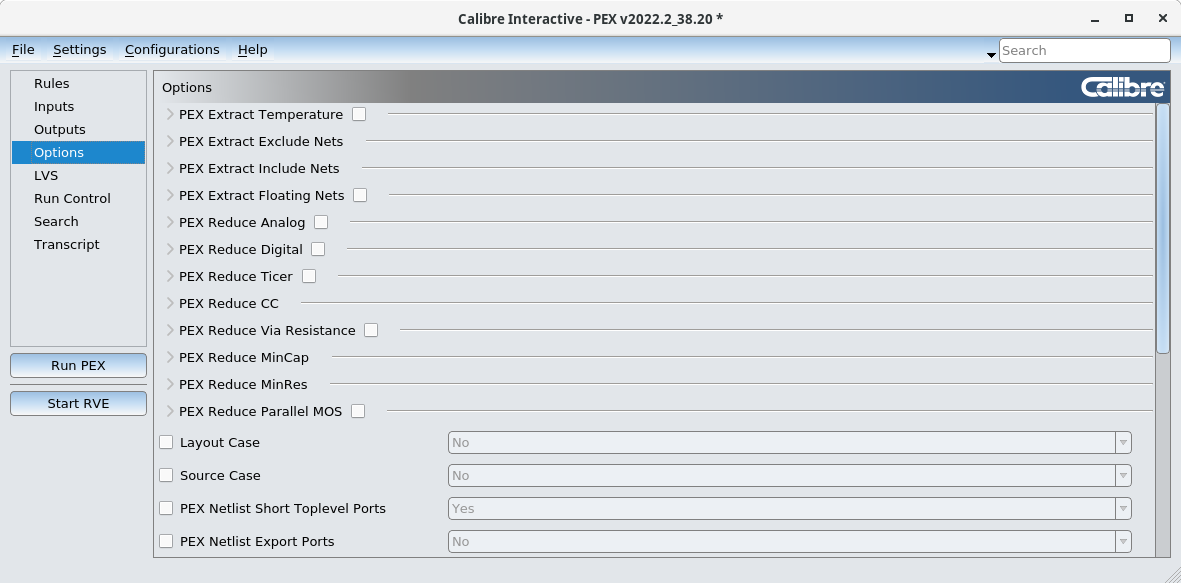
Figure 14: PEX Options.
Click "Run PEX" tab to start run PEX. Calibre view setup window opens after the run is complete.
Fill in the Calibreview setup form to generate the extracted view that can be used for post-layout simulation. Calibreview adds as an additional cellview and links to the same symbol as the "inverter" cell. Any errors or warnings during calibreview extraction will be shown on the CIW. Make sure there are no warnings and errors.
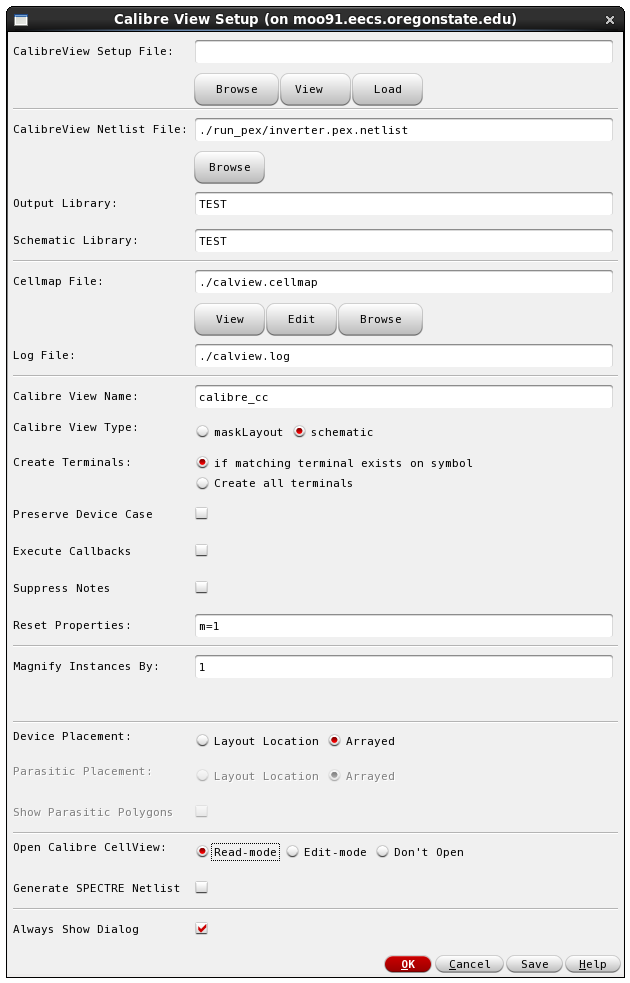
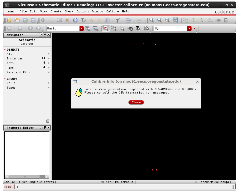
Figure 15: CalibreView Setup.
Note that LVS has to be clean for proper extraction of parasitics. Update the layout to fix the LVS errors if necessary. Click "Start RVE" tab to display PEX results. Calibre RVE displays both LVS results and the list of extracted parasitics.
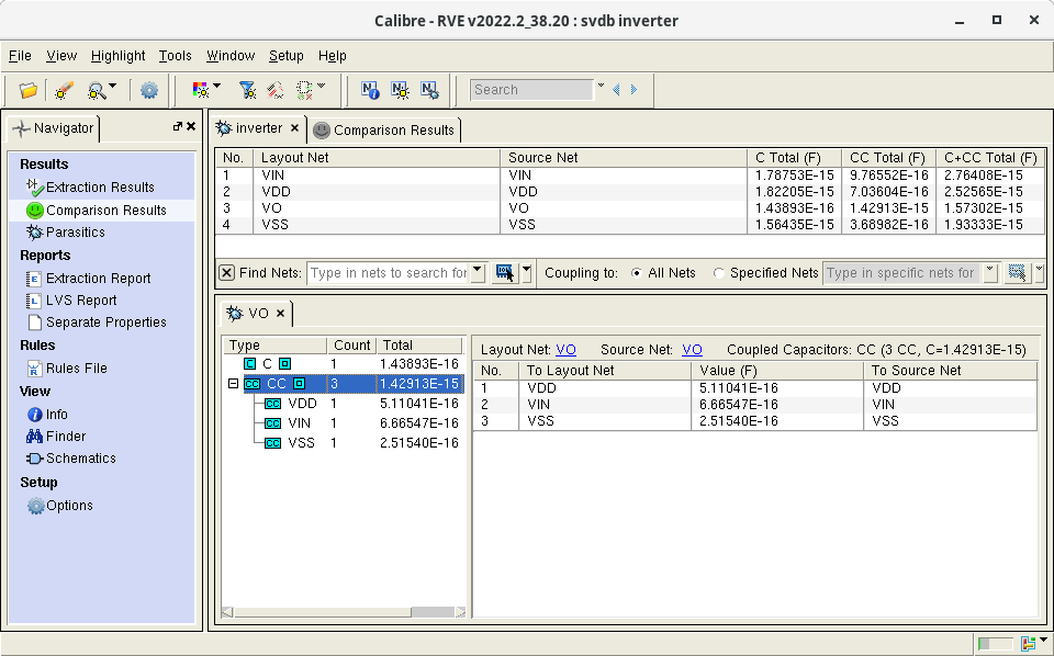
Figure 16: Calibre RVE showing Parasitics list.
Post Layout Simulation:
To simulate the extracted netlist or cell in a given tesbench, you need to create a "config" view of the testbench schematic. Note that, to perform this step you should already have a testbech schematic with the symbol of the "inverter" cell.
In Library Manager:
Highlight your library (TEST if that is what you chose).
File->New->Cellview
Choose library TEST, cell name "testbench_inverter", view type "config". Click OK.
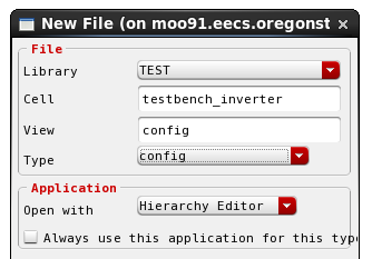
Figure 17: New Config(Hierarchy Editor) Cellview.
In the New configuration setup window, choose topcell information as Library:"testbench_inverter", View:"schematic" and click on "Use Template"
In the "Template" window choose "AMS" and Click OK. Close the New configuration setup window.
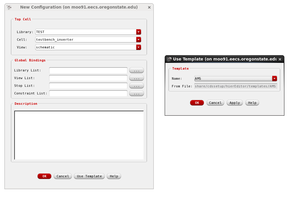
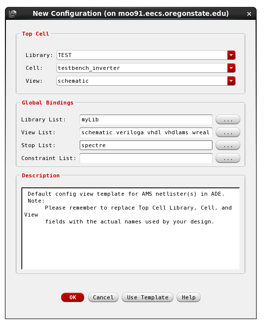
Figure 18: Config Setup.
The hierarchy editor window should now show a list of all the cells in the testbench schematic under the "Cell Bindings" tab. In this tab, you can change the inverter view to Calibre_cc view.
The hierarchy editor allows designers to simulate multiple cellviews associated with the same symbol using a single testbech. Once the required extracted calibre view is chosen, the simulation procedure is same as that of a schematic
simulation.
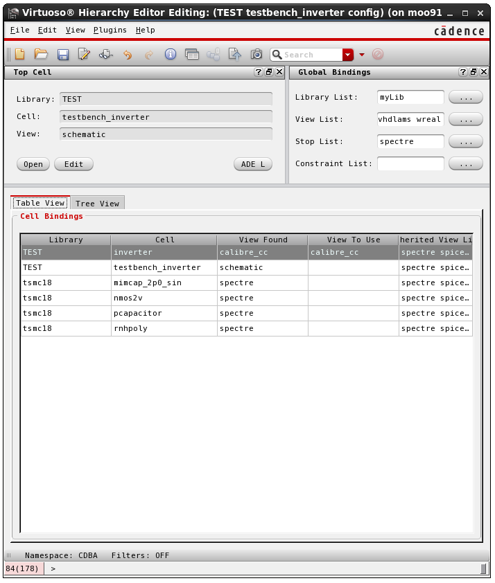
Figure 19: Hierarchy Editor.
Instantiating cells:
To make layout design more simple, it's possible to define blocks
which are to be used several times in the same layout. The following example
describes how to do this for a transistor.
Design or copy one of your transistors to a separate place. Select
the whole transistor and choose:
Edit->Hierarchy->Make cell
Fill in a name for the cell, for example, `nmos_10_1', (which stands
for w=10u and l=1u, just to keep track of what it is).
You will see the cell as a red outlined box. The contents of this box are now in
a different hierarchy level, and can only be accessed with
hierarchy commands.
This cell exists now in the library manager. To place more
copies in your layout, select:
Create->Instance
Type the name of the library, cell and view, and place it with the mouse.
You can also create arrays of cells, which can be used, for example,
to make transistors in parallel. When creating an instance, the form
gives you options to change the number of columns or rows, and the
distance between the elements.
To return one of the cells to normal layout rectangles, select the
cell and use:
Editing hierarchical designs:
When you want to edit a cell, you have to navigate between
different hierarchy levels. This is done by selecting the desired cell
and using:
Edit->Hierarchy->Descend [X]: Descends to cell.
Edit->Hierarchy->Edit in Place [x]: Allows editing while looking
at the top level.
Edit->Hierarchy->Return [B]: Returns to top level.
Of course, you can also edit the cell by opening it from the library manager.
To see all the hierarchy levels, you can use the shortcut key F. To see only
the top level, use ^f. This information can be accessed from the menu Options->Display.
In the dialog box, there is a field with the `Start' and `Stop' display levels.