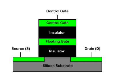
Figure 1: Representation of a flash cell. The floating gate lies between the oxide layer of the control gate and substrate [11].
In the realm of data storage technologies, the advent of Solid-State Drives (SSDs) marks a significant leap forward, providing a compelling alternative to traditional Hard Disk Drives (HDDs). This transition is not merely a change in storage media but represents a fundamental shift towards achieving greater efficiency, speed, and reliability in data storage. Amidst various innovations in SSD technology, Zoned Namespace (ZNS) has emerged as a groundbreaking development, offering a novel approach that promises to optimize SSD performance and endurance far beyond what's achievable with conventional SSD architectures.
SSDs, based on NAND flash memory, offer drastic improvements in random access speed, making them ideal for applications where quick data retrieval is critical. However, despite these advancements, the traditional architecture of SSDs, which employs a Flash Translation Layer (FTL), faces challenges such as inefficient space utilization and write amplification, impacting the SSD's longevity and performance.
ZNS comes into play as an innovative solution to these challenges. By dividing the SSD into zones with data written sequentially within each zone,
ZNS significantly reduces the overheads associated with traditional SSD management. This approach minimizes write amplification, a critical factor
in extending the lifespan of the SSD, and improves overall storage efficiency. Furthermore, ZNS aligns closely with modern storage workloads that
are increasingly sequential in nature, making it an ideal fit for contemporary data management strategies.
In essence, the introduction of ZNS in SSDs is a response to the evolving demands of data storage efficiency and longevity.
It reflects a deeper understanding of how data is accessed and managed in today's computing environments, leading to storage solutions that are
not just faster but also more attuned to the needs of modern applications and systems. The shift towards ZNS SSDs is a crucial step in the
ongoing journey to optimize data storage technologies for the future's ever-expanding and increasingly complex data landscapes.
One of the major drawbacks of the Flash Translation Layer (FTL) is the fact that a single flash cell cannot be erased individually and that an entire
block must be erased in order to erase particular data in memory. This is referred to as garbage collection. Blocks consist of pages, with each page
consisting of a specific size of accessible memory, usually around 4KB [1]. When a block is erased, both the valid data and the invalid data get erased,
and the valid data must be written to another free block in order to be preserved. This results in write amplification which is the result of unnecessary
write operations and decreases the life-span of the device. In addition to write amplification, the latency of erasing operations takes significantly
longer than write operations which slows down performance. The FTL, which runs on the SSD itself, handles all of the block management following the
specification of various schemes. From this perspective the host machines can provide random writable addresses that span the address space which
doesn't take into account the nescessary organization on the back-end to maintain the data, and the FTL has to make it work. Since the FTL cannot see
upstream to the host machine or the set of addresses that will be accessed it cannot prepare an address space that will minimize garbage collection
and write amplification.
ZNS addresses this issue by running on the host machine and by having access to the memory access patterns of host applications. This allows the ZNS
host to group data with a high probability of being erased together into the same zones, reducing write amplification [1]. The host also explicitly
controls garbage collection which can be scheduled around access to the I/O hardware which can significantly decrease the percieved latency issue with
erase operations [1]. To maximize the performance increase with ZNS, research must be done to compare the performance metrics of garbage collection
events, write amplification, wear leveling, and average latency - and others, to existing schemes using FTL and how tuning the ZNS parameters affects
the performance metrics.
Simulation and emulation tools exist to perform this type of research. Simulation will execute a large set of write and read operations on a device and
monitor the performance metrics while the executions take place. Emulation takes the current hardware of a computer system and creates a virtual machine
that runs an image. The image is essentially an operating system that is designed to use the current hardware of the host system to execute what would
be the functionality of the hardware of the emulated system. Many tools exist for simulation and some for emulation, although not without a learning
curve.
The most fundamental piece of flash memory is the flash cell. The flash cell is simply a mosfet transistor that has what is referred to
as a floating gate. This floating gate is an added layer between the gate and the substrate which can potentially hold charge. When no electrons
are in the floating gate the cell is said to be storing a "0" and when electrons are present in the floating gate the cell is said to be storing
a "1". Figure 1 shows an example of a flash cell. In order to get charge into and out of the cell an effect called Fowler-Nordhiem Tunneling is utilized. When a sufficient voltage is
applied to the gate of a flash cell, around 18 volts, electrons in the substrate can penetrate the oxide layer separating the substrate and the
floating gate, which embed themselves in the floating gate. When the voltage is removed the electrons can stay within the floating gate for years.
On the other hand when a large negative voltage is applied to the floating gate the charge in the floating gate can be injected back into the
substrate. This is how a flash cell is written and erased. In order to read the flash cell another technique is used. Typically a mosfet transistor
will have a threshold voltage that when surpassed across the gate-to-drain terminals will allow a current to flow, but with the presence of the
floating gate there is potential for a charge to already be embedded toward the gate. If there is already charge in the floating gate, then if a
slightly lower than threshold voltage is applied to the gate in reference to the drain there should still be a current that can be induced. With
current sensing hardware it can be determined whether or not the there is charge embedded in the floating gate when a slightly less than threshold
voltage is applied to the gate which is how a flash cell is read.
Figure 1: Representation of a flash cell. The floating gate lies between the oxide layer of the control gate and substrate [11].
A solid state device (SSD) is comprised of billions of individual flash cells which involve multiple levels of organization. The lowest organized
level is the page which consists of around 16Kb of cells. Pages are organized into blocks which will contain up to 256 pages.
The block is the most generally interfaced level of the SSD architecture with data being erased and written to block by block. Blocks are
organized into a plane which consist of an array of blocks, and lastly the planes are organized onto a die. This organization is shown in figure 2. Per chip there may be multiple die
and per memory module there may be multiple chips. In order to write, erase, and organize data in all of these structures typically there is a
onboard software that keeps track of all of this called the Flash Transition Layer (FTL). The FTL manages the virtual to physical address translation,
read/write operations, how and when data should be free'd from a block, among other operations.
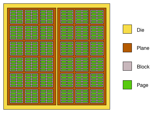
Figure 2: Representation of a flash chip. Arrays of flash cells make up a flash page while arrays of pages make up a block.
blocks are organized on planes and planes are organized on dies. There can be multiple dies per chip [12].
Since the flash cell is still a physical device, and the oxide layer that separates the substrate from the floating gate is getting punched through
by electrons on each write and erase, the flash cell has a limited lifespan. In order to maximize the lifespan the goal would be to minimize the
amount of write and erase operation's. Unfortunately, flash devices are erased on the block level, and since blocks are made up of pages which make
up a good chunk of actual flash cells, one erase operation targets a large group of cells. Since invalid data can't be overwritten in the traditional
sense, new data usually is written to another space in memory, and the old data is left in memory and invalidated. When a block fills up and more space
is needed the invalid data can't be erased, all the data must be erased. Therefore, in order to preserve the data a copy-on-erase occurs that
copies the valid data and rewrites it to another free block, as shown in figure 3. This results in something referred to as write amplification. Write amplification is the
necessary writing to a flash device due to the erasing of valid data along with the invalid data in a block. Write amplification is one major
performance metrics for SSD controller schemes and the aim is generally to reduce write amplification when possible.
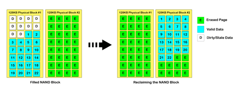
Figure 3: Updated data gets written to a new location in memory and the previous data is left in memory and invalidated [11].
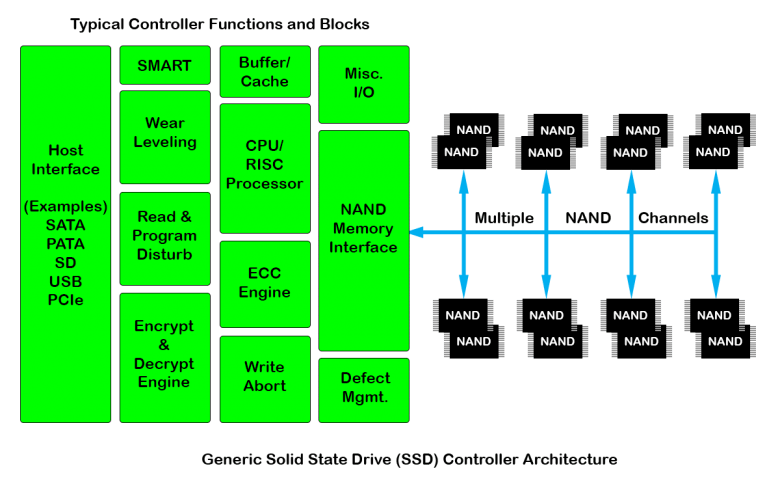
Figure 4: FTL functions in managing the physical layer of the SSD [11].
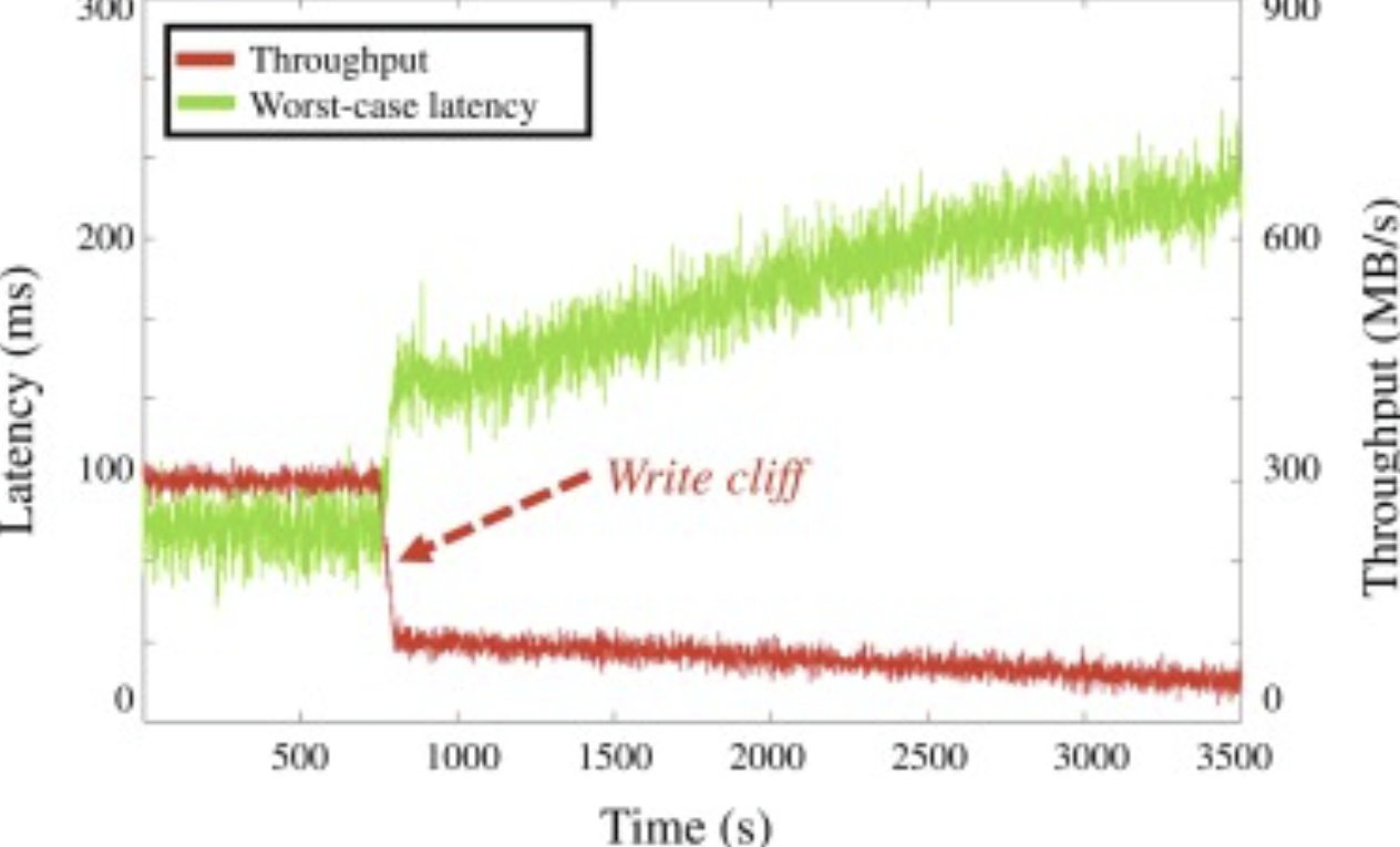
Figure 5: At about 750 seconds the SSD hits the write cliff resulting in a drop in throughput and an increase in latency [13].
The NVMe Partition Namespace (ZNS) command set is an extension of the existing NVMe (Non-Volatile Memory
Express) standard designed to optimize the way solid state drives (SSDs) manage and store data. The technology
introduces the new concept of partitioned namespaces, which is different from the traditional block-based storage
model used in SSDs. In traditional SSDs, data can be written and erased independently in small blocks, which can
lead to inefficiencies such as write amplification and the need to reserve space to maintain performance and
endurance. ZNS changes this by organizing storage space into zones, which are larger areas that must be written to
sequentially. The benefit of zones allows for programs to organize their write requests more efficiently while still allowing
the flash controller to manage the actual writing. The organization of partitioned namespaces (ZNS) in solid state drives (SSDs) represents a novel approach to data
storage that is more in line with the physical characteristics of NAND flash memory, and is designed to optimize
performance, improve storage efficiency, and extend the life of flash memory. The basic unit of
organization in ZNS is the zone. A zone is a contiguous area on an SSD that contains a set of logical block
addresses (LBAs). These zones are designed to be written sequentially, meaning that data must be added
sequentially without skipping blocks.
Typically, zones can be categorized based on their use and characteristics, such as writable zones (zones that can
be written to), read-only zones, and offline zones (zones that are not currently available). Figure 6 shows the fundamental zome
types in a ZNS SSD. Regarding writes in ZNS,
within each zone, data must be written sequentially from the beginning to the end of the zone. This constraint is
enforced to reduce write amplification and extend the life of the SSD by minimizing unnecessary erase and rewrite
cycles. ZNS provides specific commands for managing zones, including turning zones on, off, and resetting them.
This effectively manages where data is written and helps optimize the use of SSD storage capacity. On the other
hand, ZNS allows random reads within any zone, despite the sequential write requirement. This ensures that while
data must be written sequentially, it can be accessed randomly to meet the needs of various applications and
workloads without sacrificing performance. Due to this structure, ZNS has a number of benefits. By reducing the
need for over-provisioning (reserving a portion of an SSD's capacity for wear leveling and garbage collection),
ZNS allows more of the total storage capacity to be used for actual data storage. This is because the sequential
write model inherently reduces write amplification. ZNS's approach to data organization helps simplify the
wear-leveling and garbage collection process. By sequentially writing data in zones, SSDs can more easily manage
these tasks, further extending the life of the drive. Finally, ZNS also requires integration with software awareness.
To take full advantage of ZNS, file systems and applications may need to understand the partitioned storage model.
This may involve modifications to ensure that data is written in a manner that aligns with zone boundaries and
adheres to sequential write requirements.
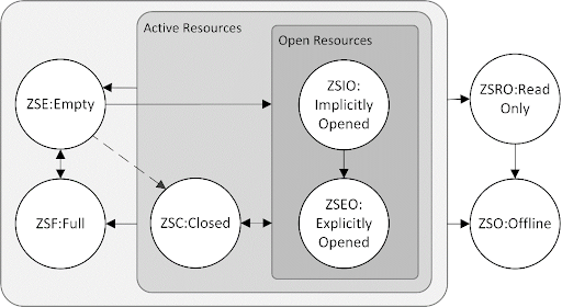
Figure 6: State machine transitions for various types of zones in a ZNS SSD [14].

Figure 7: Organizational difference between a traditional file system and a log-structured file system [15].
In ZNS, SSDs can have simpler controller
designs by shifting some data management responsibilities to the host system. For example, ZNS simplifies the
logic required for data placement, garbage collection, and wear leveling by enforcing a sequential write model
within each zone. This simplicity reduces the complexity and cost of SSD controller hardware. In contrast, SSDs
that rely on traditional FTL mechanisms require more complex controllers. These controllers must handle complex
mapping tables, garbage collection algorithms, and wear-leveling mechanisms to manage random write and read
access patterns at the block level. This complexity increases the cost of the controllers and thus the cost of the SSD
as a whole. Second, over-provisioning can be reduced on the host, using a model like ZNS where data must be
written sequentially within zones, thus inherently reducing write amplification. This efficiency reduces the need
for large amounts of reserved space, which is the practice of including additional storage capacity in the device to
manage wear leveling and garbage collection. Less over-provisioning means more of the actual SSD capacity is
available for user data, effectively reducing the cost per available GB. Traditional SSDs typically require a
significant amount of reserved space to maintain performance and endurance over time. This hidden cost adds to
the overall cost of SSDs to the end user. Finally, SSDs can be optimized for specific workloads on the host. By
allowing the host system to manage the placement of data, storage policies can be optimized for specific
applications or workloads, potentially improving performance and lowering the cost of customized use cases. On
the other hand, FTL provides a generic solution designed to be one-size-fits-all, but which may be inefficient for
specific types of workloads that could benefit from a more specialized data management strategy.
Figure 8 shows the connection between the host system and the device. The host for a ZNS SSD is connected to the device via PCIe data bus. One can imagine
an application which wants to read and write to the SSD. The application passes its requests to the kernel and the kernel sends the R/W commands to the SSD.
In an FTL system the host side sends the commands and the SSD controller then must control all aspects of how those reads and writes occur
in between all of the other management tasks the SSD controller must perform; including address mapping, garbage collection, bad block management, etc.
Now consider the ZNS system. The application initiates a R/W request to the kernel and now the kernel has control over when the R/W commands get sent
along with when garbage collection happens, where the R/W accesses are happening, how those addresses get mapped and more. All of this can be controlled
on the front end by faster processors and more RAM. When it is determined that the R/W commands should occur, the commands are sent over the PCIe bus
to the SSD who's only job is to execute those commands. The SSD works faster and the front end tasks can happen faster because the host resources are more extensive.

Figure 8: Interface between the host system and the device.
When the kernel has direct control over
how data is written to the ZNS SSD, it can optimize data placement and access patterns based on application
behavior and underlying storage characteristics. This can include aggregating small writes into larger sequential
writes, aligning write operations to zone boundaries, and efficiently managing zone resets and allocations. It also
reduces overhead, and by managing data placement at the kernel level, the system can bypass some of the
overhead associated with traditional block storage interfaces that require more complex mapping and translation
layers such as FTL. This direct control allows for more direct and efficient communication with the SSD, resulting
in reduced latency and increased throughput. By controlling data placement and write patterns from the kernel, the
system can implement effective wear-leveling strategies to extend the life of ZNS SSDs. Sequential writes within
zones minimize the need for frequent erase and rewrite cycles, which can impair the lifetime of NAND flash. Thus,
the combined effect of these aspects is that access to the ZNS address space from the kernel supports more
efficient write patterns by tightly integrating data management policies with the physical characteristics of the SSD.
This results in improved performance, reduced wear and tear on the storage media, and potentially lower overall storage
costs due to longer device life and better utilization of available storage capacity.
In traditional SSDs, the Flash Translation Layer (FTL)
handles the mapping of logical to physical block addresses, wear leveling, and garbage collection within the SSD
controller. This centralized approach can create bottlenecks because the controller must manage these tasks
sequentially or can only use limited parallel processing power due to hardware constraints. With ZNS, much of the
data management logic, including garbage collection and wear leveling, can be moved to the host (e.g., the
operating system kernel or dedicated storage management software). The host typically has more processing power
and can manage multiple tasks in parallel more efficiently than an SSD controller. Modern CPUs have multiple
cores and are capable of executing multiple threads in parallel. By moving GC and WL tasks to the host, these
operations can utilize the parallel processing power of the CPU to manage multiple zones or SSDs at the same time.
This can significantly speed up these tasks compared to being handled by the limited resources of an SSD
controller. Host-based management allows for more sophisticated and flexible data management policies that can
be customized to specific workload or application requirements. For example, the host can schedule garbage
collection and wear leveling operations during periods of low activity to minimize the impact on performance, or
tasks can be prioritized based on urgency or expected revenue. The host system can dynamically allocate resources
to storage management tasks based on current system load and priority. This means that during periods of high
demand it can prioritize application performance, while during idle periods it can focus more resources on
maintenance tasks such as GC and WL. Because the host has a global view of all storage resources and their usage
patterns, it can make more informed decisions about how to allocate writes, when to perform garbage collection,
and how to evenly distribute wear and tear across SSD memory cells. This holistic approach allows for more
efficient utilization of the SSD's lifespan. In short, by leveraging the host's powerful and scalable compute
resources, ZNS can achieve better parallelism in performing garbage collection and wear-leveling tasks. This
approach not only improves the performance and efficiency of these necessary maintenance operations, but also
contributes to longer SSD lifetimes and more consistent performance.
Figure 9 shows the throughput of a ZNS SSD and two traditional block SSD's. It can be seen that the write cliff happens
at just about 2TB of data written for the traditional block SSD's. It can also be seen that for the ZNS SSD there is no
drop in throughput at all even past the point where the capacity is filled. This provides a huge improvement over the traditional
performance.
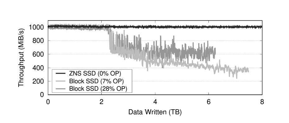
Figure 9: No write cliff in ZNS SSD due to better parallelism and timing for GC and I/O [16].
Ensures data is written sequentially within zones to comply with ZNS requirements and maximize SSD life. It has
a write buffer feature that accumulates write requests in a buffer and organizes them to be written sequentially
within zones, reducing the need for zone resets. The other, called a log-structured file system, takes a
log-structured approach to managing writes, naturally aligning with the sequential write constraints of ZNS by
treating each zone as a log.
Effective ZNS algorithms require software-level support, including modifications to the file system and storage drivers to understand and optimize the ZNS model. While the ZNS algorithm is primarily software-driven, its efficiency and effectiveness can be enhanced by hardware features designed to support ZNS operations, such as SSD controllers optimized for sequential zone management. The development of ZNS algorithms is an active area of research, with ongoing efforts to refine zone management, data placement, and wear-leveling strategies to better utilize the benefits of ZNS SSDs. This includes exploring new file system designs, storage management techniques, and application-level optimizations to take full advantage of the sequential write and random read capabilities of ZNS.
One proposed scheme for ZNS is called ZNS+ which was announced at the USENIX Symposium on Operating Systems Design and Implementation in 2021.
ZNS+ is a log-structured file system aware ZNS design that supports internal zone compaction (IZC) and sparse sequential overwrites. ZNS+ targets
F2FS as the log-structured file system to implement its ZNS+ aware system ontop of. F2FS divides chunks of its address space into hot, warm,
and cold segments. Hot sections are then copied and appended into cold sections to facilitate wear leveling.
IZC improves the performance of the LFS by removing all the invalid stored memory in a zone [10]. Typically compaction requires a victim
segment selection, destination block allocation, valid data copy, and meta-data update [9]. In a regular ZNS scheme the host would be
responsible for controlling these operations. The ZNS+ scheme provides an additional NVMe command zone_compaction that allows the SSD to
handle the valid data copy. This streamlines the copy process by eliminating the need for the host to copy data from the SSD and then write
it back, by allowing the SSD to internally copy without data transfer through the bus.
Sparse sequential writes are essentially writing short bursts of sequential data. In a non-ZNS file system sparse sequential writes can be
converted to dense sequential writes (which are what ZNS requires, zone level sequential writes) by filling in the gaps between the sparse
writes with other data to join the sparse sections together into a dense sequential section. This is called threaded logging, although because
going back and filling gaps in the written data does not conform to the sequential writing specification of ZNS, direct threaded logging cannot
be done. What is proposed in ZNS+ is that spare sequential writes can be padded with valid data from victim blocks until new writes occur,
called internal plugging. This allows for efficient garbage collection to happen and for smaller bursts of write traffic to be serviced which
will result in a more consistent throughput [9]. The internal plugging is proposed to be done completely on the SSD to reduce latency and
maximizing throughput over the PCIe bus for host to device writes.
The copyback features allows for data migration from block to block as long is it is on the same chip. This is already implemented as a feature
in SSD's and is incredibly useful for garbage collection. ZNS+ proposes copyback-aware block allocation to ensure copyback operations are used
to move data from blocks free'd from garbage collection to new blocks on the same chip.
Mapping a zone to flash blocks allows a zone to be filled in such a way that the host can write to different zones depending on the address
space accessing them. One technique proposed by ZNS+ is to map multiple flash blocks from multiple chips onto one zone. In this mapping, chip
level parallelism can be used. The flash block groups must be interleaved such that all the block offsets on the parallel chips are equal. The
set of logically consecutive blocks across parallel chips is called a stripe. The number of flash chips involved in the interleaving is called
the zone interleaving degree. The zone interleaving degree for a zone can be less than the total number of chips as long as it is an equal
divisor of the total number of chips such that all the flash block groups are equal size and distributed across all the chips. The divisions
are then called flash chip groups [9].
eZNS, where the "e" stands for elastic, adapts the current ZNS model which currently only supports static zones. The problem is proposed that
after a zone is allocated and initialized, its maximum performance is fixed regardless of the underlying device capability, its I/O configurations
cannot adapt to runtime workload characteristics, and cross-zone I/O interference yields unpredictable I/O executions [17]. eZNS explores stripe
configuration in terms size and width, zone placement across channels and dies, I/O scheduling to avoid write buffer overflow and interference on a die.
Recall, that stripes are zones that cross multiple planes and dies such that the blocks in each plane can be interleaved and accessed in parallel.
What eZNS implements is a zone arbiter and an I/O scheduler that sits on top of the NVMe driver. The zone arbiter dynamically changes zone sized based
on need, and avoids overlapping zones, by utilizing the v-zone structure interface. The v-zone interface is shown in figure 10. The I/O scheduler manages read requests using delay-based congestion control strategies and manages write requests
by using a token based admission control [17].
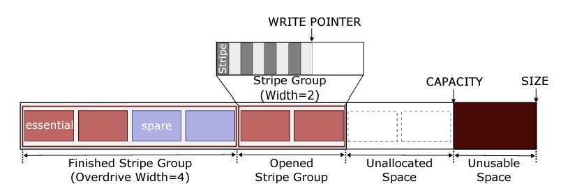
Figure 10: V-zone structure used by eZNS to dyanmically change the zone size at run-time [17].
In order to quantitatively represent the benefits one scheme may have over another an accurate and reliable testing environment must be used. In
the case when testing hardware we not only need simulations in order to replicate potential workloads, but we may need emulation in order to model
hardware using software. Emulation is especially useful when physical prototypes are expensive or when the physical prototypes have a limiting
lifespan, both of which are the case for SSD's.
DiskSim is an open-source C based simulation environment developed at University of Michigan and enhanced at Carngie Mellon University. It is a
highly accurate simulator that includes modules for storage components, buses, drivers, controllers, and adapters [2].
Historically the simulator was designed for HDD simulation, but in 2009 Microsoft developed a SSD extension that allowed for SSD simulation in the
DiskSim environment [3]. DiskSim is limited to internal storage simulation however, and does not allow for interfacing with the host
device for splitting workload tasks which makes it unsuitable for ZNS research.
FlashSim was developed with SSD's in mind and is object oriented in nature, written in C++. This allows for better scalability to larger systems
with more flash chips and flash controllers. Specifically, FlashSim has simulation of the FTL in mind but is designed to be integrated with DiskSim.
In that sense, while it is flexible it is also limiting and runs into the same issue as DiskSim by not being able to shift control to the host.
One benefit of FlashSim compared to other flash simulators is the ability to run multiple schemes of FTL including page-based, block-based, FAST,
and DFTL [4].
Open-channel SSD's are SSD's that lack a firmware layer that manages the block interface. The host is entirely able to, and required to provide the
functionality of address mapping, garbage collection, wear leveling and other features of the flash layer. In terms of research this is a good thing
because it gives full control over the implementation schemes, and it can be integrated to the application level, kernel level, or post-kernel level
allowing the most flexibility for developing control schemes. Although Open-channel SSD's are gaining popularity due to the necessity to expose
the memory architecture, they still remain expensive and the barrier to entry still exists for the typical user who must know how to configure their
kernel to allow for an open-channel controller and deploy effective control schemes for their workloads [5].
Cosmos+, which superceeded Cosmos, is a hardware PCIe based SSD platform developed on the HYU Tiger4 SSD controller and is developed at Hanyang
University, Korea [6]. The board is an FPGA and uses a subset of NVMe and is used for memory architecture exploration in a real system.
NVMeVirt is a recent software based flash emulator presented at the FAST'23 conference. It uses a modified Linux kernel image installed into a
virtual machine which modifies how the kernel interfaces with the memory. The way the interfacing happens is entirely configurable based on the
type of flash memory system and scheme being used. Due to its interaction with the kernel on the virtual machine this tool allows for host level
control of some aspects of what the controller would typically do. Because of this NVMeVirt is capable of emulating ZNS, NVMe, and traditional SSD
devices. [7]
FEMU is a flash emulator tool first presented at FAST'18 and similarly to NVMeVirt, it also uses a modified Linux kernel image to run on a
QEMU virtual machine. FEMU itself emulates the flash controller and can insert itself into various levels of the controls tack depending on
what mode it is operating in. Blackbox mode operates with FTL on the device with no visibility to the way the devices is managing its
address mapping, garbage collection, wear leveling, and other features. Whitebox mode transports the FTL onto the host device, which allows
for the host to read and write commands in a manner that align with the control scheme and operates essentially as a virtual open-channel
SSD. NoSSD mode allows for simulation of as-fast-as-possible SSD's such as Intel Optane and Z-NAND SSD's. Lasty, ZNS mode exposes the
NVMe Zone Interface which allows for read and write operations that follow the ZNS command set [8].
FEMU was used to model and simulate a ZNS SSD and some information about the system, how it works, and how to set it up will be discussed in this section.
In order to set up FEMU we first needed to download both the FEMU source code from github, linked here, and the
custom kernel to emulate the ZNS SSD must be obtained. This is available for free by following the steps listed on the github page and contacting the lab at
Univerity of Chicago. There is a walkthrough on setting up the environment on their page and that will not be discussed here.
Once the FEMU code has been built and QEMU is installed, the custom kernel is extracted and ready to be mounted and the script to run the kernel in ZNS
mode can be run. The script can also be modified to change the parameters of the SSD. Inside the script "run-zns", the following parameters can be found
and edited; SSD_SIZE_MB, NUM_CHANNELS, NUM_CHIPS_PER_CHANNEL, READ_LATENCY_NS, WRITE_LATENCY_NS. The actual script is shown in figure 11. Changing these
parameters requires a rebuild of the FEMU code.
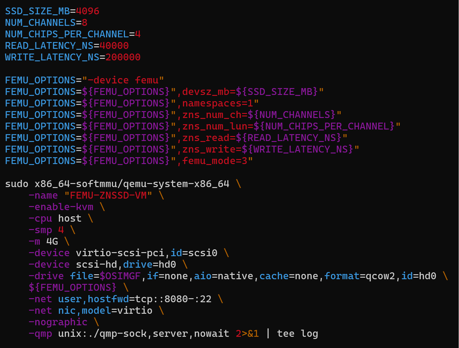
Figure 11: run-zns script inside the build-femu folder in FEMU.
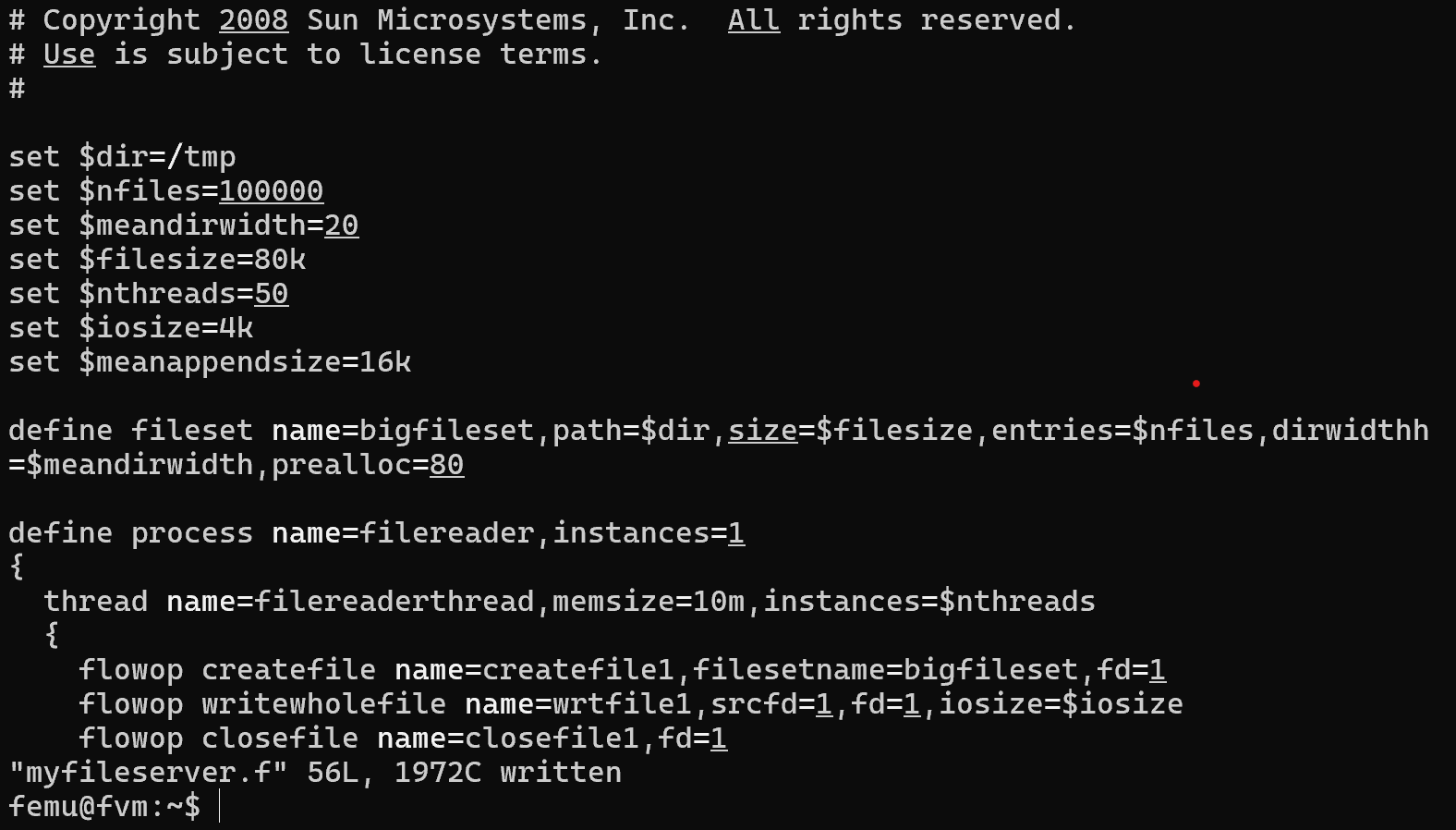
Figure 12: Filebench Simulation File.

Figure 13: Result of filebench workload on the emulated SSD.
Some challenges were encountered when setting up the simulation and emulation environment. Mainly, there wasn't much documentation on how
to actually use FEMU once it was installed. It also doesn't include any scripts for evaluating the performance of the SSD or any sort of metrics on
the garbage collection events, write amplification, and wear-leveling. Using filebench was helpful because it did provide some information about throughput
during its workload, although the default script does not provide fine grained detail on the throughput as a function of time or data written.
Firstly, we would like to learn how to use filebench to provide the fine grained throughput information, as the functionality is there but time did not
allow for that in the scope of this project. We would also like to explore other R/W workload simulators to see what capabilities they have and gain
some variety to the simulation results.
Next we would like to gain access to a more robust version of FEMU. The group that wrote ZNS+ also put out their custom kernel and build environment to
reproduce their results. The custom kernel contains evaluation scripts that give details on the garbage collection, write amplification, and zone compaction
metrics. An example of the output of their evaluation script is shown in figure 14. Originally, we tried to use this to do the simulation but the custom kernel required 34GB of RAM for the virtual machine. We did not have access to
a machine with this much RAM that we could use for this project. They also provided the kernel code with the ability to modify the kernel to require less RAM to
emulate the system. We tried to adjust the kernel size requirement and rebuilt the kernel using BusyBox but ran into issues when booting the new kernel on QEMU.
We would like to get into the custom kernel provided by ZNS+ and see how they structured and integrated their evaluation scripts in order to implement our own
evaluation scripts.
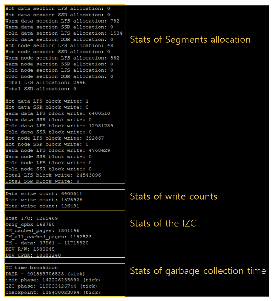
Figure 14: Evaluation script from ZNS+ custom FEMU build [9].
Daniil Lytikov - ZNS Survey Research
Qunyi Pan - ZNS Survey Research
Sean Bullis - ZNS Survey, Emulation, and Simulation Research
[1] T. Stavrinos, E. Katz-Bassett, D. S. Berger, and W. Lloyd, HotOS,
in HotOS '21: Proceedings of the Workshop on Hot Topics in
Operating Systems, 2021
[2] G. Ganger, "The DiskSim Simulation Environment (V4.0),"" Parallel Data Laboratory, https://www.pdl.cmu.edu/DiskSim/index.shtml
(accessed Feb. 21, 2024).
[3] "Download SSD extension for DiskSim simulation environment from official Microsoft Download Center,"" Microsoft Store - Download
Center, https://www.microsoft.com/en-us/download/details.aspx?id=52332 (accessed Feb. 21, 2024).
[4] Y. Kim, B. Tauras, A. Gupta, and B. Urgaonkar, "First International Conference on Advances in System Simulation," 2009
[5] "Open-Channel Solid State Drives," openchannelssd.readthedocs.io, https://openchannelssd.readthedocs.io/en/latest/ (accessed Feb. 21, 2024).
[6] J. Kwak, S. Lee, K. Park, J. Jeong, and Y. H. Song, "Cosmos+ OpenSSD," ACM Transactions on Storage, vol. 16, no. 3, pp. 1-35, Jul. 2020. doi:10.1145/3385073
[7] S.-H. Kim et al., "Empowering Storage Systems Research with NVMEVIRT: A comprehensive nvme device emulator,"" ACM Transactions on Storage,
vol. 19, no. 4, pp. 1-26, Oct. 2023. doi:10.1145/3625006
[8] H. Li et al., "USENIX Conference on File and Storage Technologies," in University of Chicago, 2018
[9] K. Han, H. Gwak, D. Shin, and J.-Y. Hwang, "ZNS+: Advanced Zoned Namespace Interface for Supporting In-Storage Zone Compaction,"" in Proceedings of
the 15th USENIX Symposium on Operating Systems Design and Implementation, 2021
[10] S. Podeti, "Log Compaction and Merging,"" Medium, https://medium.com/@sureshpodeti/log-compaction-and-merging-9b2e0ffca690 (accessed Mar. 6, 2024).
[11] S. Larrivee, "Solid state drive primer # 1 - the basic NAND flash cell," Cactus Technologies,
https://www.cactus-tech.com/resources/blog/details/solid-state-drive-primer-1-the-basic-nand-flash-cell/ (accessed Mar. 16, 2024).
[12] "Understanding flash: Blocks, pages and program / erases," flashdba, https://flashdba.com/2014/06/20/understanding-flash-blocks-pages-and-program-erases/ (accessed Mar. 16, 2024).
[13] J. Boukhobza and P. Olivier, "Flash Translation Layer,"" in Flash Memory Integration, Elsevier, 2017, pp. 129-147
[14] "NVM Express" Zoned Namespace Command Set Specification Revision 1.1d, 2023. Accessed: Mar. 12, 2024. [Online].
Available: https://nvmexpress.org/wp-content/uploads/NVM-Express-Zoned-Namespace-Command-Set-Specification-1.1d-2023.12.28-Ratified.pdf
[15] T. Bao, "Log structured file system for dummies,"" {Tinou Bao}, https://work.tinou.com/2012/03/log-structured-file-system-for-dummies.html (accessed Mar. 16, 2024).
[16] M. Bjørling et al., "ZNS: Avoiding the Block Interface Tax for Flash-based SSDs ZNS: Avoiding the Block Interface Tax for Flash-based SSDs,"
[17] J. Min, C. Zhao, M. Liu, and A. Krishnamurthy, "eZNS: An Elastic Zoned Namespace for Commodity ZNS SSDs," in Operating Systems: Development and Implementation, Accessed: Mar. 07, 2024.
[Online]. Available: https://pages.cs.wisc.edu/~mgliu/papers/eZNS-osdi23.pdf