MOSIS NDA
This is an important step to obtain access to tsmc 0.18um pdk for the class
To access tsmc 0.18um pdk, mosis requires all the users to sign a Non-Disclosure Agreement (NDA).
Please print a copy of the MOSIS NDA
form, sign and submit to Prof. Moon to be added to the pdk user list.
EXAMPLE:
DESIGN AND SIMULATION OF AN INVERTING AMPLIFIER
This example will help you familiarize with Cadence OA. You will design
a simple inverting amplifier, and then observe its operating
point and frequency response behavior.
This will show the most important commands and steps to use when working
with schematics in Cadence.
Before starting with the design example, there are some details
that are worth mentioning:
- The appendix contains some notes about using the on-line help feature,
and using the mouse. There's also a table with keyboard shortcuts.
- Most of the commands in Cadence can be accessed in multiple
ways: pull-down menus, shorcut keys, buttons in toolbars, etc.
In the described example, all the commands are referenced by
their position in the pull-down menus.
- The most used key in Cadence is ESC. It is used to cancel
on-going commands.
The following picture shows the inverting amplifier circuit, ready for
netlisting. The next section explains how to draw it in Cadence.
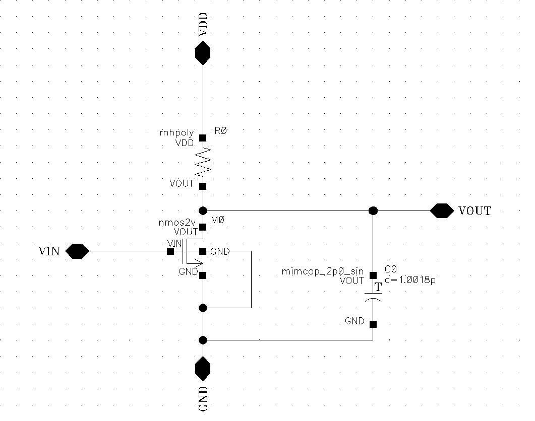
Figure 1: Design example.
You may see license warnings about Virtuoso_Schematic_Editor_L or Analog_Design_Environment_L in the CIW window. You may ignore this. That just means the basic license for Schematics L or ADE L is unavailable, and another version called Virtuoso_Schematic_Editor_XL or Analog_Design_Environment_GXL will be used.
1. Create a library for your new design:
>From the library manager window:
File->New->Library
Type a new name, such as TEST. Click OK
In the dialog box "Technology File for New Library", choose "
Attach to an existing technology library".
Then from the dropdown menu choose "tsmc18".
Click OK
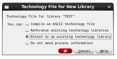
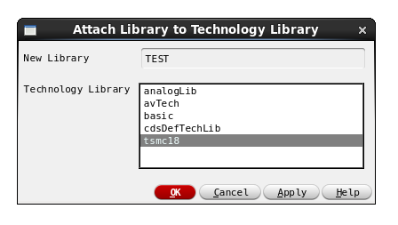
Figure 2: Attaching Technology Library.
2. Create a new cell, where you will design the inverter:
In Library Manager:
Highlight your new library (TEST if that is what you chose).
File->New->Cellview
Choose library TEST, cell name "inverter", view type "schematic". Click OK.
Figure 3: New Cellview.
A schematic window will open.
3. Design your circuit:
3.1 Placing components:
For this inverter, you will need an nmos transistor, a resistor and a capacitor.
>From Schematic window:
Create->Instance
In the Add Instance window Click Browse to open Component Browser.
Make sure the Library in the Component Browser is set to tsmc18 and enable Show Categories to sort the components in the pdk library.
In the Component Browser window,
For mosfet, choose
Category: Mosfet_4T
Cell: nmos2v
View: symbol
then place it.
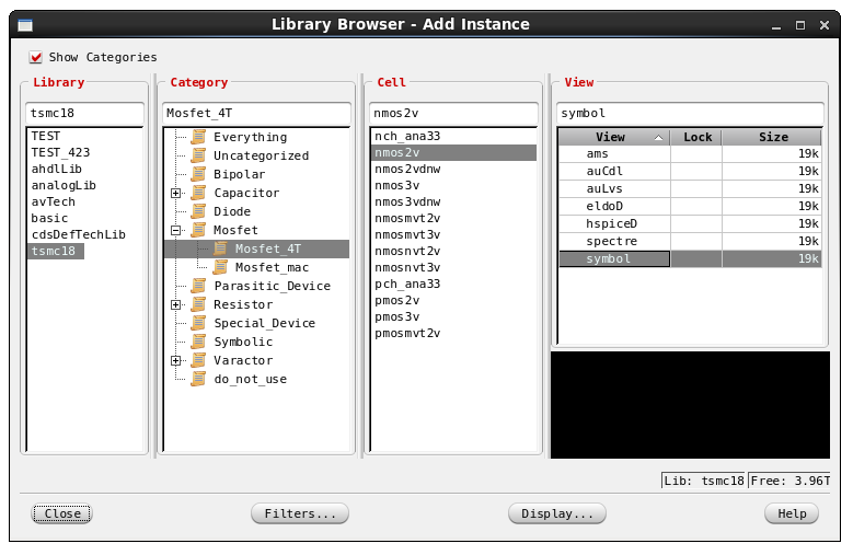
Figure 4: New Instance: Mosfet.
Use the same procedure to place resistors (rnhpoly) and capacitors (mimcap_2p0_sin)
from library tsmc18.
For resistor, choose,
Category: Resistor_2T
Cell: rnhpoly
View: symbol
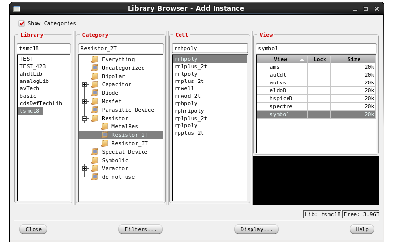
Figure 5: New Instance: Resistor.
For capacitor, choose,
Category: Capacitor_BB
Cell: mimcap_2p0_sin
View: symbol
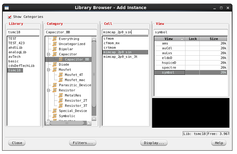
Figure 4: New Instance: Capacitor.
If you make any mistake, you can always use:
Edit->Delete or
Edit->Rotate or
Edit->Move or
Edit->Stretch
You need to change the properties of some components:
Edit->Properties->Objects
Select the transistor, and change the following parameters:
Length (l): 1.2u
total_width: 60u
Fingers: 5
NOTE: For this design kit you can only set transistor lengths and widths
in multiples of grid units(.005uM). Keep this in mind when making your circuits.
Select the resistor. Edit the segment width and segment length properties to set a resistance of 4k Ohms.
The resistance value is given by R = sheet_resistance*(segment_length/segment_width). For rnhpoly, the sheet resistance is 295.3 ohms/square.
Select the capacitor. Edit the Width and Length properties to set a capacitance of 1pF.
The capacitance value is given by C = Capacitance_per_unit_area*(length*width). For mimcap_2p0_sin, the capacitance per unit area is 2fF/um2.
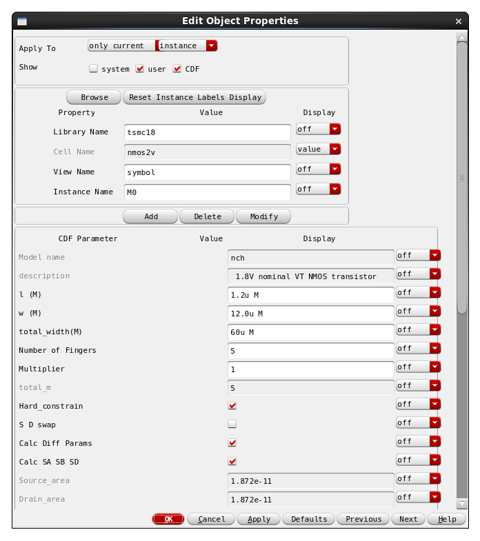
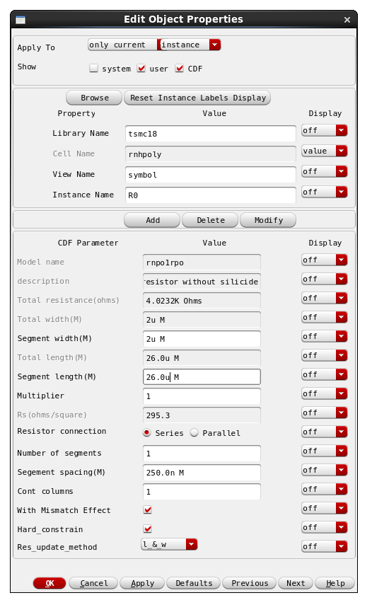
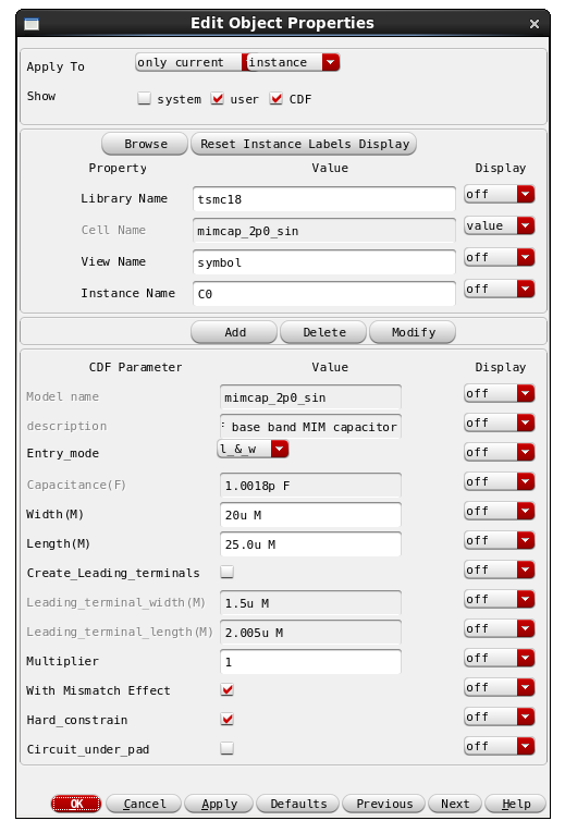
Figure 5: Instance Properties.
3.2 Connect components:
Connect the component terminals as shown in figure 1, using:
4. Adding Pins:
By adding pins, you can identify the I/O ports of the schematic. At a later stage, you can
also use pins as connection points for hierarchical designs. To learn more about this, see
the section about creating symbols.
Create->Pin
Type the pin name, such as VIN, select the direction as "inputoutput", and
place it in the schematic.
Do the same for VOUT
, VDD and GND, select the direction as "inputoutput".
5. Simulate With Spectre:
This section explains how to simulate in Cadence using Spectre. Create a new cellview called "testbench_inverter" and instantiate the symbol inverter into the testbech. Add supply and input voltage sources.
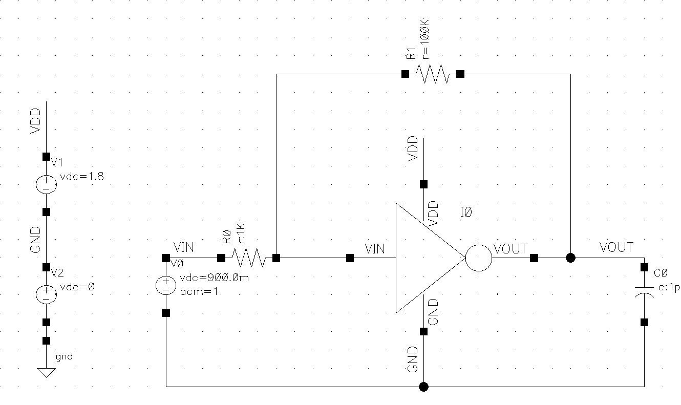
Figure 6: Testbench.
To run the simualtion, launch the Analog Design Environment (ADE) window from:
Then, in ADE Window:
Setup->Simulator/Directory/Host
Set the simulator to "spectre".
Set the Project directory where the simulation files will be saved.
To change the process corners from typical(tt) to slow(ss) and fast(ff) corners:
Setup->Model Libraries. Edit the "sections" field:
For mosfets, change "tt" to "ff" or "ss".
For mim capacitors, change "tt_mim" to "ff_mim" or "ss_mim".
For poly resistors, change "tt_res" to "ff_res" or "ss_res".
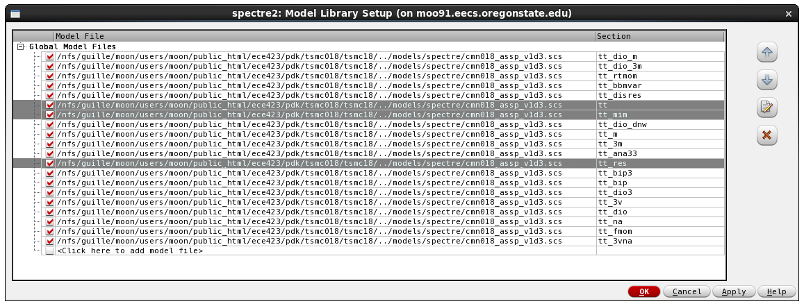
Figure 7: Changing Process Corners.
To setup dc and ac simulations:
Under the Analyses section-> Click to add analyses.
Under dc, choose "save dc operating points" and click "enabled" checkbox.
Under ac, setup the sweep variable as frequency and choose the sweep range for the simulation.
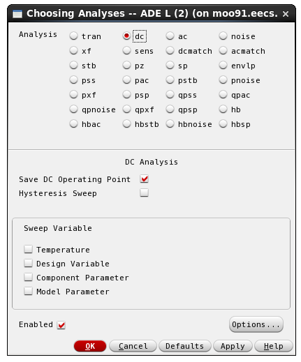
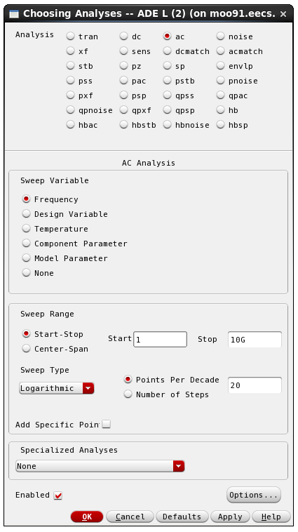
Figure 8: DC and AC Simulation Setup.
To run simulation:
Simulation-> Netlist and Run. Or click on the green play button on the right side of the ADE window.
To run a simulation with a variable sweep:
Add design variables to setup by right clicking on Design Variables in the setup section -> Copy from Cellview
Choose the variable and modify the design variable as required. Variables can be defined by specifying specific values as a list. Aternatively, as a sweep from initial to final value with step size
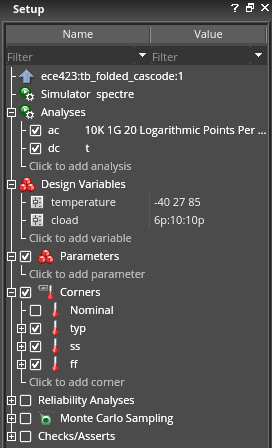
Figure 9: Variable Sweep Setup.
To run multiple corner simulations for your test:
Corners -> Click to add corner
Define typical, slow and fast corners by adding design variables and defining the temperature and vdd.
Model groups can be created to simulate process variation effects. Separate model files need to be included for each model group to simulate specific corners.
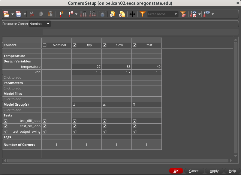
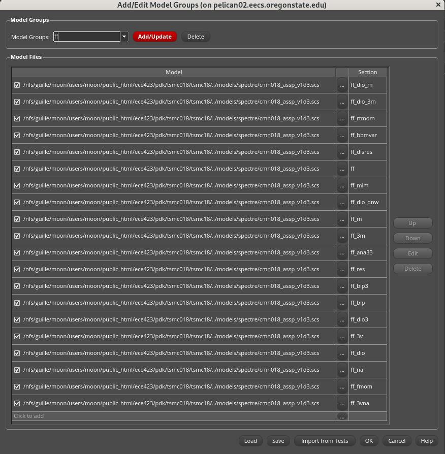
Figure 10: Corner Setup and Model Group.
To save the cellview and rerun some other time:
File-> Save.
The test bench gets saved as a maestro view. To reload the saved test bench, navigate to the the cell in Library Manager and open up the saved maestro view.
6. Simulate With Hspice:
If you know how to use these tools or would like to play with them, please feel free to try. If the integrated simulation environment works for you, then great - you will not need to do the steps in this section or the following one (View Results). However, as a backup, you should try be comfortable with exporting the netlist manually, simulating with hspice from the command line, and viewing the results in an external viewer. This procedure is explained in this section and the next...
It's possible to generate a
complete netlist from the schematic and to simulate it outside the
Cadence tools environment.
Invoke the Analog Environment simulation window from:
Launch->ADE L
Then, in ADE Window:
Setup->Simulator/Directory/Host
Set the simulator to "hspiceD".
Generate netlist:
Simulation->Netlist->Create
The netlist is displayed in a special window. Use the menu
File->Save As to save it in your work directory. Let's
name it 'inverter.sp'.
Note that this will save the netlist in the Cadence directory that you
created in the Starting Design Framework II step. If you wish to save
it to a different location, you must enter the complete target path
(beginning from root).
You can now simulate this netlist file with HSPICE. But before you do, it's necessary to
add some more things. With your favorite editor, open the file and add the following components:
Vdd vdd! 0 DC 5V

Vin vin 0 DC 0.75 AC 1
Also, Ddefine a dc operating point and an ac analysis with the following:
.AC DEC 10 1e3 1e9
To simulate for different process corners edit the line that includes the "hspice.mdl" file.
For typical corner (tt):
.INCLUDE "/nfs/stak/users/moon/ece423/pdk/tsmc018/models/hspice/hspice.mdl"
For slow corner (ss):
.INCLUDE "/nfs/stak/users/moon/ece423/pdk/tsmc018/models/hspice/hspice_ss.mdl"
For fast corner (ff):
.INCLUDE "/nfs/stak/users/moon/ece423/pdk/tsmc018/models/hspice/hspice_ff.mdl"
Finally, you need to remove the following line:
.OPTION INGOLD=2 ARTIST=2 PSF=2 PROBE=0
... and to replace it with:
.OPTION POST
Now you can start the simulation:
hspice inverter.sp >! inverter.lis
If everything goes well, you will get the message 'hspice job concluded'.
Otherwise, if something goes wrong, you will get 'hspice job aborted'.
6. View Results:
For Spectre simulations, you can view results by using the Results menu in the ADE. Explore the Direct Plot, Print, and Annotate sub-menus. To see DC node voltages, operating conditions, etc, use the options in Restuls->Print or Results->Annotate. For waveforms, look in Results->Direct Plot.)
For Hspice simulations,
You can see the DC operating point by opening the file inverter.lis with
a text editor, and searching for the keyword 'mosfets'. The node voltages can be found if
you search for the keyword 'operating'.
To see the frequency response, you will have to use a graphic postprocessor, such
as CosmosScope:
- Start CosmosScope from the unix prompt (just type 'scope').
- In CosmosScope window, select File->Open->Plotfiles, and
under the 'Files of type' menu select HSPICE. Navigate to the
correct directory and select the
file inverter.ac0.
- In the window that opens, you will see a list of
nodes
to plot. Double-click on the node Vout.
- To zoom, click and drag on either axis. The Tools->Measurement
Tool is also very useful and intuitive. You may print the plot with
File->Print.
- Before you print, change the the background of your plots from black to white.
This is done by Graph->Color Map->Mono.
This completes the simulation, and the design example.
Most things in Cadence tool are intuitive, so I hope this tutorial gave you
a good feeling for its environment. Feel free to explore the menus
and capabilities of the tools you just used.