This is an important step to obtain access to tsmc 0.18um pdk for the class
To access tsmc 0.18um pdk, mosis requires all the users to sign a Non-Disclosure Agreement (NDA).
Please print a copy of the MOSIS NDA
form, sign and submit to Prof. Moon to be added to the pdk user list.
WORKING WITH SYMBOLS
If you want to use your design in other schematics, you need
to create a symbol for it.
This is equivalent to the use of subcircuits in HSPICE. It gives
a hierarchy to your project, making it easier to organize.
Creating a new symbol
First, in your schematic, remove any superfluous components that
you have used in the previous example for the simulation (vdc for the
power supply and for the input signal). These components will be defined again later.
Assign input and output pins (if you have not already done so):
Create->Pin
Type the pin name, such as VIN, select the direction as "inputoutput", and
place it in the schematic.
Do the same for VOUT
, VDD and GND, select the direction as "inputoutput".
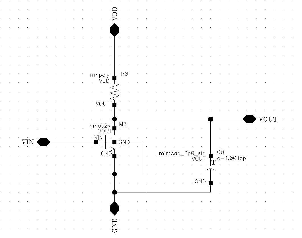
The schematic will look like this:
Figure 1: Inverter schematic with pins.
As a side comment, note that the net names changed and have now the same name as
the pins. There are other ways to name the nets. You can find
more about it in the FAQ.
Next, create the symbol:
File->Check and Save
Create -> Cellview->From cellview, click OK.
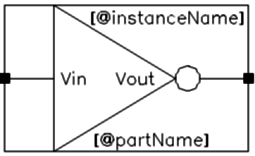
A new window will open with the symbol view.
By default, the symbol shape is a rectangle, but we can change it. Since this
design is an inverter, we will draw a triangle and put a small circle at the output.
To do this, use:
Create->Shape
There are several shapes available: line, rectangle, circle, etc.
You will want to delete the green rectangle, draw the new shape, and move
the terminals to new positions. The editing commands are similar to what
you had for the schematic window.
You will also need to change the Selection box (the red rectangle), which
defines the limits of the symbol. This can be done automatically by:
Create->Selection box
A window appears with only one button: "Automatic". Click it
and the selection box will automatically adjust to the limits of
your symbol.
Don't forget to check and save. The symbol may now look like this:
Figure 2: Inverter symbol.
You can now close the Symbol Editing window. It wont be necessary anymore.
Using the symbol in other schematics
Create a new schematic, using the instructions described in
Create a
new cell. Give a name such as test_inverter.
You place this symbol in the new schematic in the same way that
you placed any other components, with:
Create->Instance
This time changing the Library to your library and clicking on Uncategorized. Your symbol should be here.
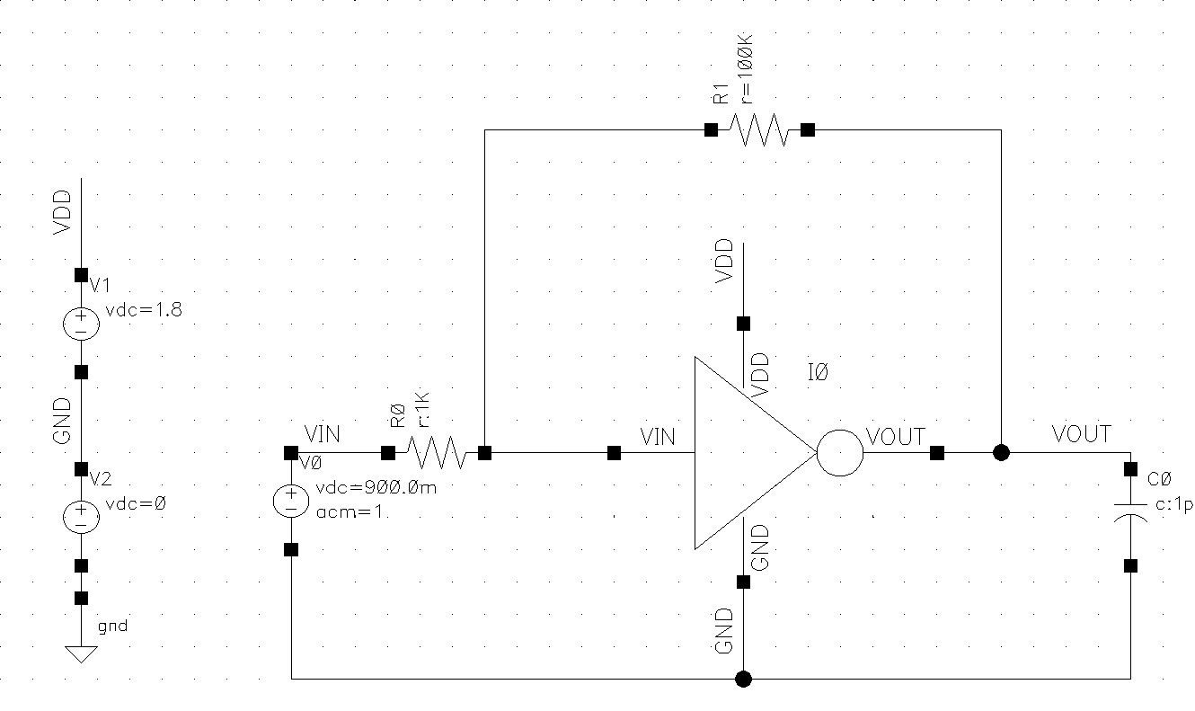
Now, you can define power supplies in the new schematic. If you place
new vdd and gnd components, they will be implicitly connected to the correspondent
vdd and gnd components that are inside the inverter.
For simulation, you can connect a 'vdc' to the input terminal of the inverter,
and a capacitor at the output terminal.
Here is an example of a possible setup:
Figure 3: Using the inverter symbol in a new schematic.
To move in the hierarchy, select the inverter, and then:
Edit->Hierarchy->Descend Edit
You can choose the schematic or the symbol for editing.