|
Home |
|
Research |
|
Teaching |
|
Publications |
|
Facilities |
|
People |
|
Openings |
|
Group Blog |
|
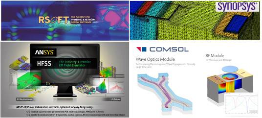
Photonic Design and Simulation: * Rsoft V8.3RC5 design suite including BeamProp, Fullwave, Bandsolver, ModeProp, Diffract-Mod and FemSim, which can provide accurate design and simulation for photonic integrated circuit devices * Comsol 4.3b for wave optics and RF& microwave simulation * RF and microwave design software: Ansys HFSS V15 * Synopsis Medici for semiconductor device simulation (Materials and Devices Group) * Other design software accessed through the School of EECS and the College of Engineering includes: Solidworks, Cadence and Matlab. * Advanced simulation workstation HP Z400 with Xeon quad-core micro-processor and 24GB memory, which can provide enormous computation power
|
|
Optical Scattering Method to characterize liquid droplet diffusion from Inkjet Printer |
|
Thermo-reflectance Method to characterize thermal diffusivity of thin film |
|
Fig.1 Simulation tools in the PI's lab for integrated nanophotonic devices |
|
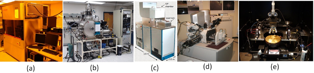
Fig.2 Some fabrication facilities for nanophotonic |
|
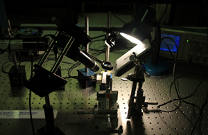
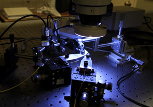
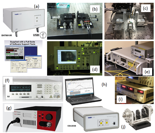
Fig.3 Optical Characterization equipment for nanophotonic devices |
|
Fabrication Facilities: * The Owen Cleanroom at OSU has campus-shared photolithography facilities and thin-film deposition systems, including direct write laser lithography [Fig.2 (a)] and contacting photolithography to create micro- and nano- scale devices. Other commonly used fabrication facilities, such as electron beam metal sputtering [Fig.2 (b)], thermal evaporation, and plasma-enhanced chemical vapor deposition (PECVD) system are also available. Particular, we recently acquired an Oxford Plasmalab System100 ICP380 [Fig. 2 (c)] for metal etching through the sponsorship of Murdock Foundation. * The Electron Microscopy Facility (EMF) provides advanced electron microscopy instrumentation services to OSU research communities. The facilities include FEI TITAN 80-200 TEM/STEM with ChemiSTEM Technology, FEI QUANTA 3D dual beam SEM-Ebeam lithography/FIB [Fig.2 (d)], FEI NOVA NanoSEM 230 high resolution SEM, and Leica DM 5000 computerized fluorescence optical microscope * The REL 4800 Probe station with thermal control [Fig.2 (e)] |
|
Device Characterization Facilities in Dr. Wang's Research Lab: * Lab space: three optical characterization labs (Dearborn 206, Dearborn 302A, Owen 333) with more than 1,500 square feet; one shared wet-chemical lab (Dearborn 302) with more than 1,200 square feet * Optical Testing Tables * Three large (10' x 4') floating optical tables with vibration isolation * Four floating optical breadboard tables (5' x 3') * Optical Coupling System * Thorlabs APT NanoTrak Auto-alignment Controller [Fig. 3 (a)] * Thorlabs Max311D 3-Axis NanoMax Stage, Closed-Loop Piezos [Fig.3 (b)] * Surface-normal optical coupling system for grating coupler or nanoantennas [Fig.3 (c)] * Multiple Thorlabs and Newport 3-axis, 4-axis, and 5-axis alignment stages * High-Speed Optoelectronic Characterization * Agilent 86100A digital communication analyzer with 86109A optoelectronic module (30GHz optical and 40GHz electrical bandwidth) [Fig. 3(d)] * HP 8510C Network Analyzer (45 MHz- 50 GHz) (shared facility at Microwave Lab) * 10GHz LiNbO3 intensity modulator * Thorlabs 818-BB-35 12.5GHz photodetector & APD310 high gain detector * Laser & Light Sources: * Carlmar femtosecond pulsed fiber laser: 0.1ps pulse, 20mW [Fig. 3(e)] * HP 8168A tunable laser [Fig. 3 (f)] * Newport 2010M tunable DFB laser: 1.48-1.62 μm * Newport 5-channel DWDM laser array at C-band * Thorlabs broadband IR ASE diode laser: 1.5-1.6 μm * NKT super-K compact light source (400-2400nm wavelength) [Fig.3 (g)] * Thorlab S9FC1004P semiconductor optical amplifier * Two Mellis-Griot HeNe lasers: 632.8 nm, 5mW * SDL CW high power CW fiber laser: 1112nm, 10W * LSI DLM-220 dye laser: 514nm, 3ns pulse * Three Nd:YAG lasers: 1064 nm and 512 nm, 10W * Avantes white light source: vis-IR * Intralux fiber optic illuminator * Various semiconductor laser diodes and LEDs * Photodetectors and power meters: * VIC silicon photomultiplier * Two Thorlab InGaAs fixed gain photodetectors * Thorlab BP209-IR beam profiler (900-1700nm) * Newport PMKIT power meter: 0.1nm-2W * Thorlab fiber-optic power meter: 800-1700nm * Thorlab USB PM100 power and energy meter with Si and Ge detectors * Optical spectroscopy equipment: * Thorlab OSA203 Optical spectrum analyzer (1.0-2.6μm) [Fig. 3 (h)] * Ando AQ6317B optical spectrum analyzer (0.4-1.7 μm) * HP70951 optical spectrum analyzer (0.6-1.7 μm) * Ocean-optics USB2000 UV-VIS spectrum analyzer * Three Chromex scanning monochromators * Electronic equipment: * Three Princeton Applied Research lock-in amplifier, and one Stanford Research amplifiers up to 250MHz [Fig. 3 (i)] * Fluke 1GHz function generator, multiplex Tektronix function generators * Three Tektronix digital oscilloscopes * Dual channel Wavetek synthesized arbitrary waveform generator * Standford Research 4-channel pulse and delay generator * 1500V voltage supply * Misc. equipment: Various fiber splitters, Thorlabs PCFFB1550Bench Fiber-optic polarizers [Fig.3 (j)], attenuators, and isolators, Fabry-Perot interferometer |