Research Areas
Our research interests are primarily focused on bringing novel electronic platforms to applications in chemistry, biology, and medicine. This work has spanned a variety of interdisciplinary fields, including CMOS integrated circuits, embedded systems, microfabrication, immunochemistry, and chemical sensing. Previous and ongoing research interests include:
Light and Dark - HDR Optical Sensors and CMOS-Integrated SPADs
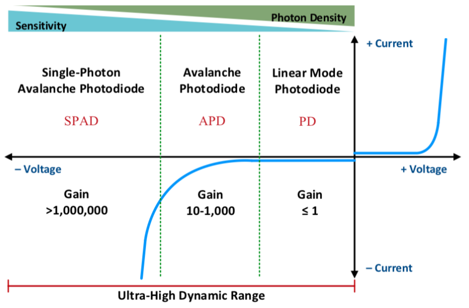
Optical sensing with visible light is used broadly across scientific applications, where its utility as a non-invasive measurement technique is essential for medical, environmental, and life sciences applications. In this body of work, we use single-photon avalanche photodiode (SPAD) devices to extend the dynamic range of conventional CMOS optical sensors. |
|
Our work has explored the combined use of single-photon avalanche and linear-mode operation regions in a single photodiode at the pixel level to provide very wide optical dynamic range. With this approach, CMOS-integrated optical detectors can be used seamlessly from very dim light to very bright light for a variety of imaging and biosensing applications. | 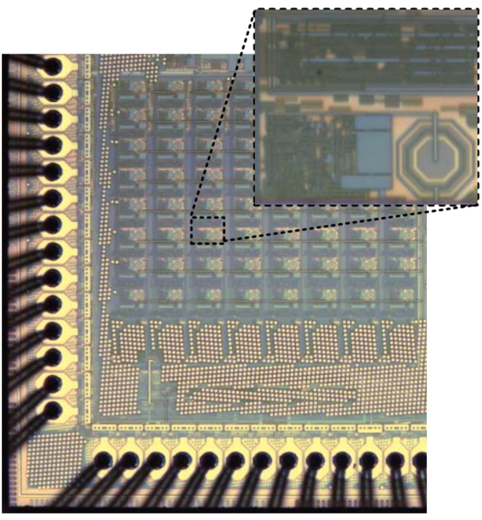 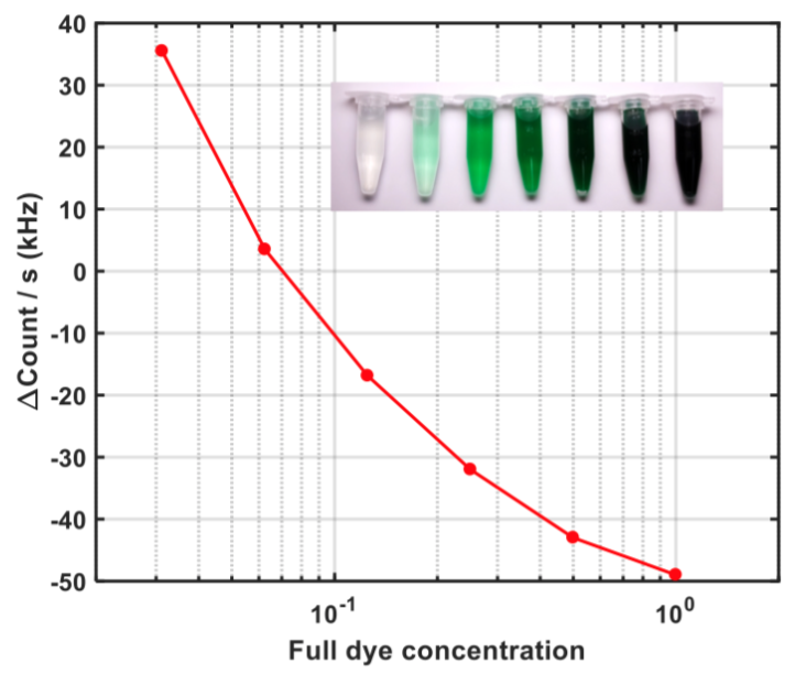 |
Electronics without Batteries - Thermoelectric Energy Harvesting
Harvesting energy from human body heat provides a ubiquitous source of energy for wearable sensors and electronics. Thermal energy can be converted to electrical energy using thermoelectric generators (TEG), solid-state devices that generate a voltage from an applied temperature gradient using the Seebeck effect. A wearable form factor requires small-area TEGs, which generate only tens of millivolts from the temperature difference between the skin surface and the ambient environment. |
|
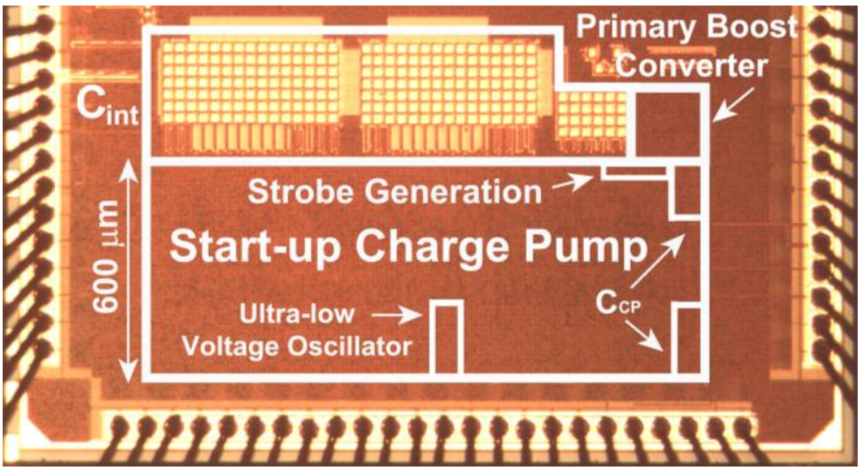
We are interested in developing thermoelectric energy harvesters for body-worn electronic sensors and systems. Toward this end, we have focused on two specific technical challenges faced by low input voltage DC-DC converters: (1) cold start, where the harvester must start without battery assistance at low input voltage (<100mV); and (2) operating efficiently at this low input voltage. The long-term goal is to enable true battery-less operation of low-power electronic devices using thermal energy harvesting. | 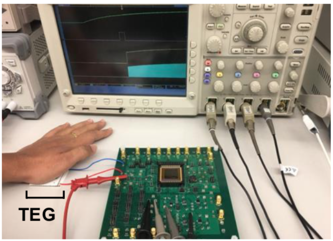 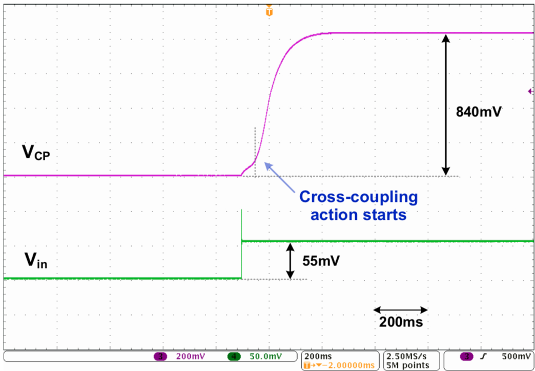 |
Stretchable Electronics - 3D-Printed Wires for Deformable Circuits
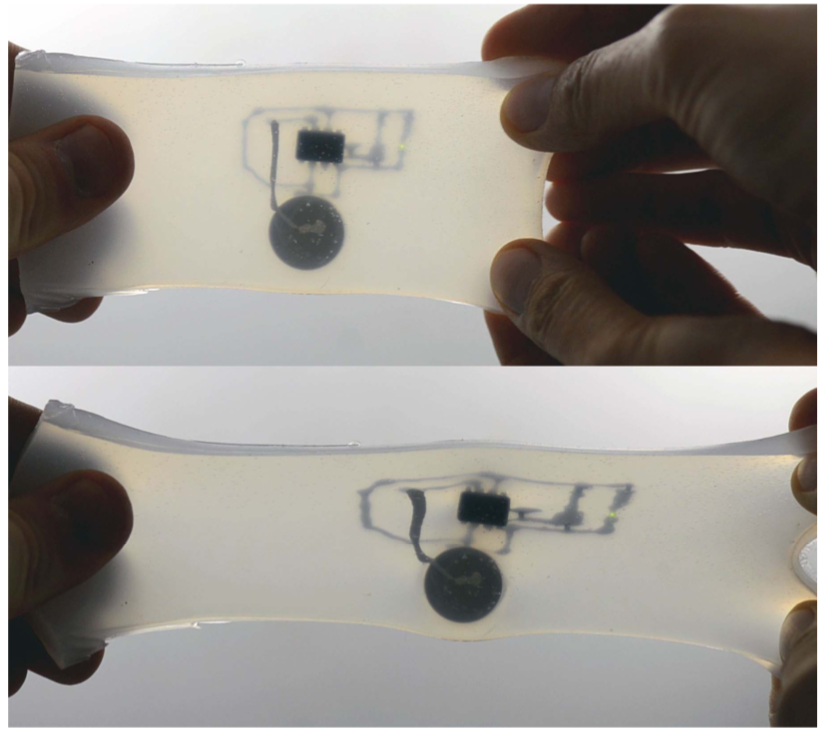
Stretchable electronic circuits and systems will be critical for future wearable devices and smart textiles, where existing fabrication approaches severely limit conformal deformation. This is especially true for wearable sensors and actuators for IoT and conformable electronic skins and textiles, all critical for emerging physical human-machine interfaces. From a packaging perspective, the basic structure and function of a rigid PCB has changed little in the last 50 years; advances such as flexible circuit boards allow deformation, but these do not provide stretch or fundamentally alter traditional 2D circuit topology. |
|
In this body of work, we use a 3D-printed liquid metal paste material to build stretchable electrical interconnects between electronic components. This approach allows us to build multi-layer "stretchable PCBs," and it provides the ability to print sensors and passives using the same material. | 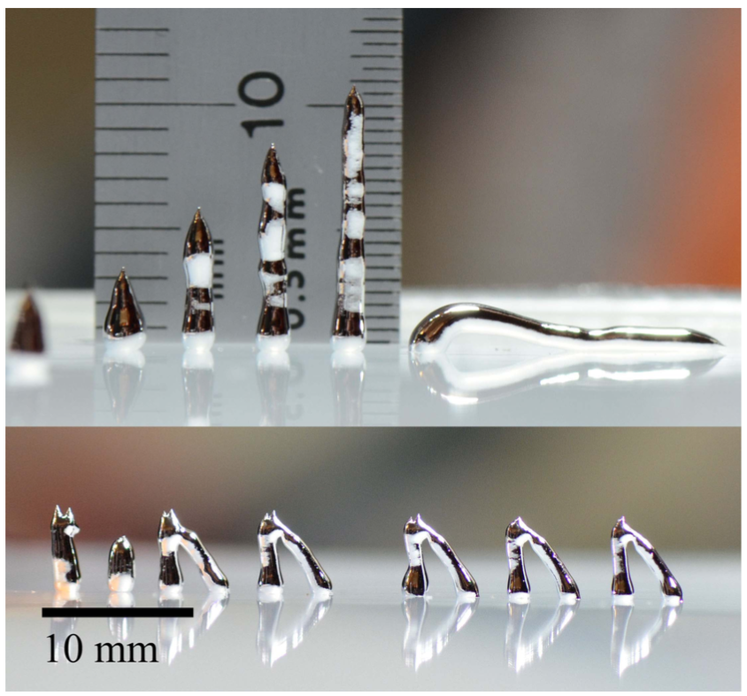 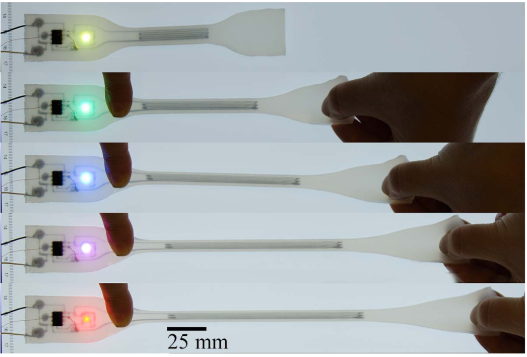 |
Lab-on-CMOS - Microfluidics over IC Sensors
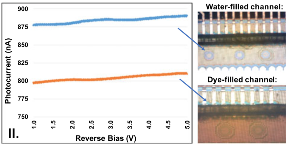
Direct sensing in liquids using CMOS-integrated optical and electrical sensors is attractive for lab-on-chip applications, where close physical proximity between sample and sensor can obviate optical lenses, enhance electrical sensitivity, and decrease noise due to parasitics. However, controlled delivery of fluid samples to the chip surface presents an ongoing challenge for lab-on-CMOS development, where traditional wire-bond packaging prevents integration of planar microfluidics. |
  |
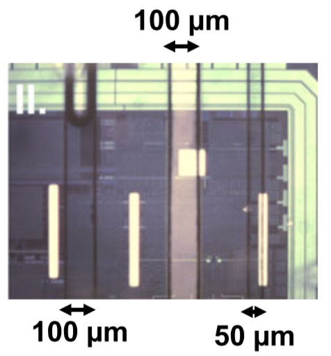
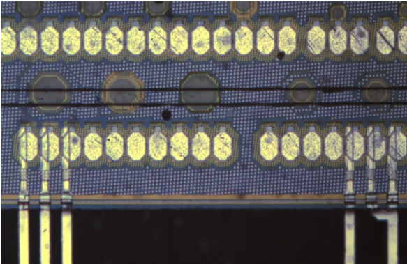
We have developed a method for scalable heterogeneous integration of microfluidic channels and silicon-integrated circuit substrates using a commercial fan-out wafer-level packaging approach. The use of compression molding enables embedding one or more individual IC chips in-plane with the surface of a uniform-thickness epoxy wafer, with minimal seam discontinuities. Once packaged, wafers allow for post-fabrication using standard semiconductor processing techniques, including photolithography and physical vapor deposition. This approach enables seamless metal routing to one or more IC dice, and it provides a continuous flat surface for microfluidic integration using traditional planar approaches. |
   |
Accessible Bio-instrumentation
At the core, we are interested in the incorporation of novel materials and devices with mixed-signal CMOS integrated circuits to fundamentally improve sensitivity, throughput, and portability of electronic sensing platforms - with a special emphasis on ubiquitous sensing, point-of-care technologies, and accessible instrumentation. |
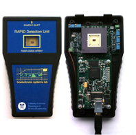 |
Label-free Sensing - Monolithic FBAR-CMOS Resonators
Traditional chemical and biological assays rely on secondary reporters for detection of binding events, as with the use of fluorescent reporters for microarrays or colorimetric enzyme labels for immunoassays. These techniques add cost and complexity to assays, provide only end-point interrogation, and often limit multiplexed detection. A move towards real-time, label-free assays provides many advantages. |
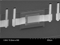 |
Broadly, we are interested in the incorporation of novel materials and devices with mixed-signal CMOS integrated circuits to fundamentally improve sensitivity, throughput, and portability of electronic sensing platforms - with a special emphasis on ubiquitous sensing, point-of-care technologies, and accessible instrumentation. As an example, we have previously employed on-chip piezoelectric resontators to build an array label-free sensors with a simple, digital interface. This has been employed in real-time sensing of volatile organic compounds (VOC), and ongoing work is aimed at adapting such sensors for use as biosensors for proteins and nucleic acids. | 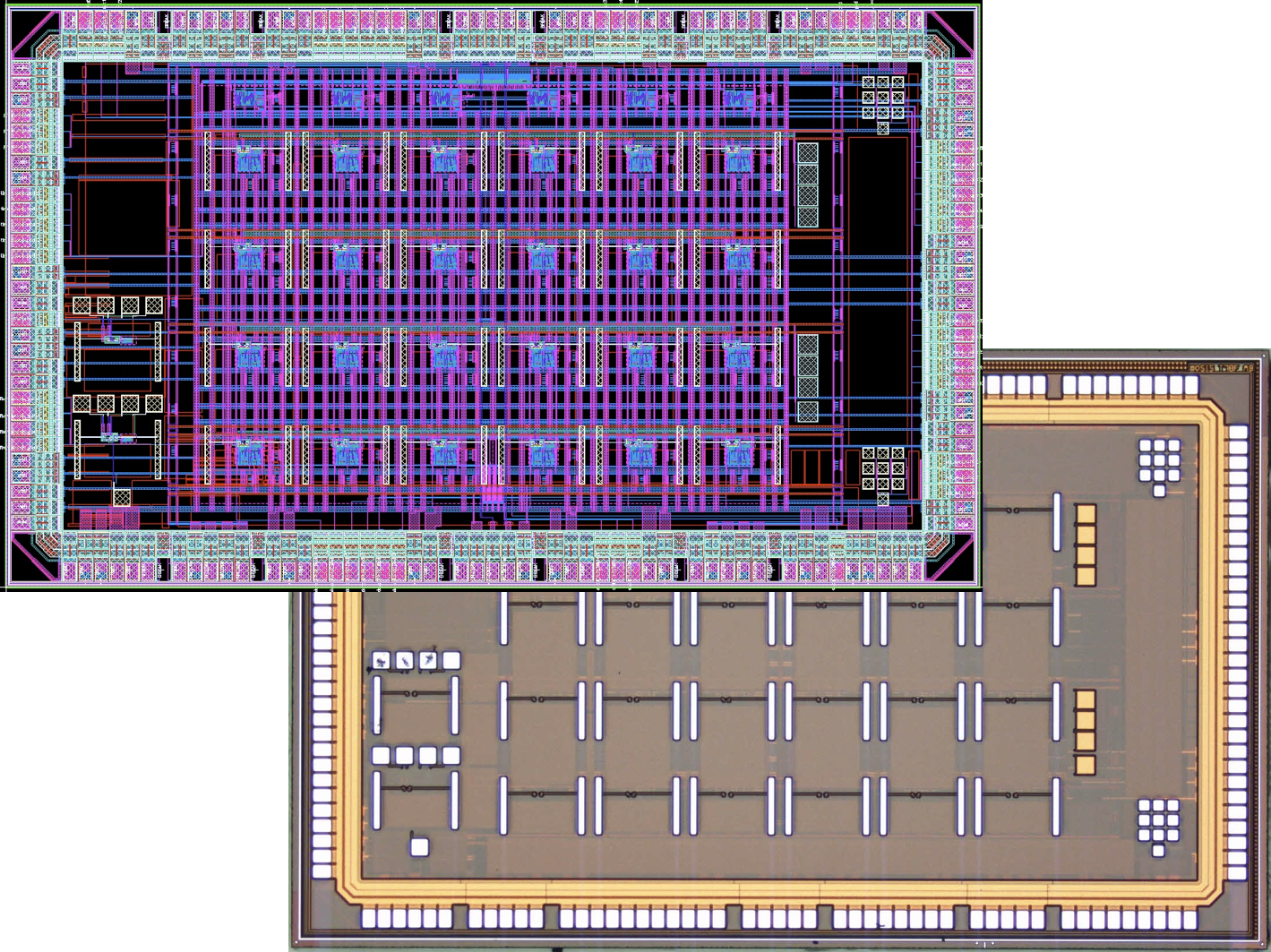 |
Radiation Detection and Dosimetry
Current strategies for minimally-invasive biodosimetry rely on the establishment of centralized testing centers with high-throughput assay processing. Patient samples must be collected and transported to a testing center, with transportation networks often compromised alongside a nuclear accident. A point-of-care biodosimetry platform would allow on-site dose quantitation, facilitating appropriate medical triage and emergency management. This is a critical and unmet need for the preparation and response to a nuclear release event. |  |
Novel Structures and Thermal Control in Microfluidics
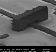
Microfludics have become an established, critical component of lab-on-chip and micro-total-analysis systems. These techniques have been employed both academically and industrially for control and routing of small fluid volumes. |
 |
