Conley Group Emerging Materials and Devices: Facilities
Electrical Engineering and Computer Science | Materials Science | Oregon State University
RESEARCH
TEACHING
CV
PUBLICATIONS
PEOPLE
FACILITIES
STUDENT OPPORTUNITIES
HIGH SCHOOL OUTREACH
SENIOR DESIGN & HONORS PROJECTS
SUPPORT
HAVING FUN
IN THE NEWS
Group WIKI
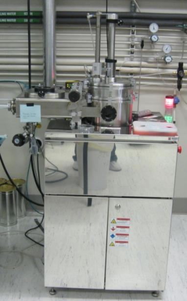
Atomic Layer Deposition (ALD) Chambers
1) Picosun SUNALE R-200 200mm Plasma Enhanced ALD system: The R-200 system is load locked, can handle 200 mm wafers, and is capable of both thermal ALD, and plasma-assisted ALD (PEALD), and is equipped with O2, H2, and N2 plasma. In addition to an H2O/O2 source line, the tool has three metal-organic source lines (one room temperature source and two heated sources for low vapor pressure precursors). Depositions at up to 500 C are possible. In-situ characterization includes a multi-wavelength ellipsometer in the load-lock, an SRS RGA 200 residual gas analyzer, and a quartz crystal microbalance (QCM).This system is also equipped for UV enhanced ALD and microwave enhanced ALD.
2) Arradiance Gemstar ALD system (see press release): 150 mm ALD reactor with 3D substrate capability, thermal ALD with H2O as an oxygen source or H2S as a sulfur source. There are four metal-organic source ports and substrate heat is available up to 475 C. The outlet valve on this tool may be closed in order to perform a 'soak' of the sample with each precursor pulse, useful for coating highly porous materials. An in-situ quartz crystal microbalance can be installed, 5 precursor source lines (1 gas; 2 vapour draw for liquids; and 2 low vapor pressure sources, heated up to 120C, one with N2 boost).
3) Picosun SUNALE R-150B: Load locked 150 mm thermal ALD system with H2O and ozone (O3) generator. In addition to the H2O/O3 line, there are four metal-organic source lines with two Picosolid Boosters heated sources (heated up to 150C), and two Picosolution precursor sources held at room temperature (Peltier cooled). Deposition temperatures from 50-400+ C are possible. System equipped with an SRS RGA 200 residual gas analyzer.
4) Anric AT200M+: Equipped with plasma and microwave enhanced ALD (MW-ALD).

ALD Materials:
Conductive
- Ru (Ru(DMBD)(CO)3 / O2)
- RuO2 (Ru(DMBD)(CO)3 / O2) - Thermal ALD & PEALD
Dielectric
- Al2O3 (TMA / H2O) - Thermal and PEALD
- HfO2 (TEMA-Hf / H2O)
- SiO2 PEALD (Bis(DiEthylAmino)Silane (BDEAS) / O2 plasma)
- Bi2O3 (Bi(OCMe2
iPr)3 and H2O)
- Nb2O5
(Nb2(OC2H5)10 / H2O)
- Ta2O5 ( Ta2(OC2H5)10 / H2O and TaCl5 / H2O)
- TiO2 (TiCl4 / H2O or Ti-tetraisopropoxide / H2O)
- ZrO2 (TEMA-Zr / H2O)
Semiconductor
- SnO2 (TDMA-Sn / H2O)
- ZnO (DEZ / H2O)
-NiO (Ni(tBu2DAD)2 / O3)
- Co3O4 (Co(Cp2) / O3)
Sulfides
- ZnS (DEZ / H2S)
- MoS2 (MoCl5 / H2S)
Various nanolaminates
Under development:
- Metal oxides, nanolaminates, and multicomponent films
Electrical Test
Four fully equipped probestations with standard Agilent I-V and C-V characterization equipment; hot chuck; cryo-probe available.
Unique Characterization Techniques
1. BlueSpin low field electrically detected magnetic resonance (EDMR) for spin dependent tunneling (SDT) and spin dependent recombination (SDR).
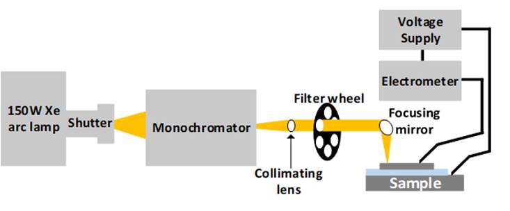
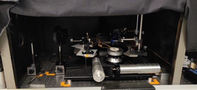
2. Internal photoemission (IPE) spectroscopy for measuring internal energy barrier heights at metal/insulator, metal/semiconductor, and insulator/semiconductor interfaces.
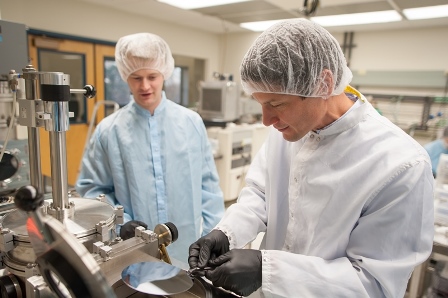
Semiconductor Fabrication
Standard sputtering deposition, evaporation, etch, clean, lithography, anneal, etc. available in co-located OSU cleanroom.
Ellipsometry, profilometry, glovebox, Kelvin probe
Nanowire Growth Systems
1) Owen System: Two zone vacuum furnace with MFC gas flow control of N2 and O2, separate tubes for carbonization of photoresist and parylene CVD
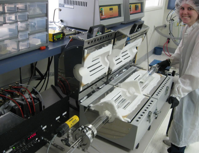
2) Kelley System: Two zone atmospheric furnace with MFC gas flow control of N2 and O2
See OSU Materials Synthesis and Characterization (MASC) Center Website:

Analytical
Spectroscopic ellipsometry, atomic force microscopy (AFM), x-ray diffraction (XRD), x-ray reflectivity (XRR), x-ray photoelectron spectroscopy (XPS) are available in shared use facilities on campus.
OSU Electron Microscopy Facility: Transmission electron microscopy (TEM), scanning electron microscopy (SEM),
Miscellaneous
Other analytical support available through ONAMI facilities such as CAMCOR, CEMN, and EMIF
Probostat