Conley Group Emerging Materials and Devices: Outreach
Electrical Engineering and Computer Science | Materials Science | Oregon State University
RESEARCH
TEACHING
CV
PUBLICATIONS
PEOPLE
FACILITIES
STUDENT OPPORTUNITIES
HIGH SCHOOL OUTREACH
SENIOR DESIGN & HONORS PROJECTS
SUPPORT
HAVING FUN
IN THE NEWS
Group WIKI
High School Outreach
Summer Experience in Science and Engineering for Youths - SESEY
Summer 2011
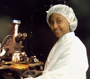 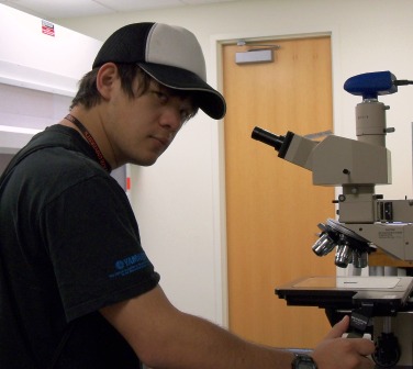 |
Yadano Kumbi (top) Xavier Artache (bottom) Yadano and Xavier assisted in the fabrication and characterization of MIS devices. They helped to use atomic layer deposition (ALD) and thermal evaporation to fabricate the device. They then determined the size of the devices using a microscope. Thicknesses and IV and CV data were then obtained to determine the dielectric constant of the devices. |
Summer 2010
 |
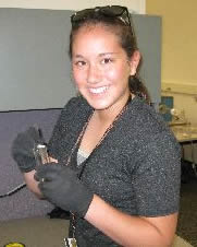
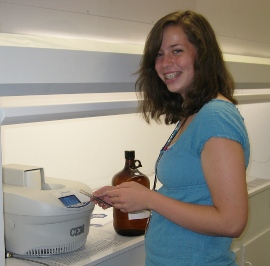
Penelope Biggs (left) Marie Pahlmeyer (right) Marie and Penelope assisted in the growth of zinc oxide nanowires. Working in a cleanroom, they also helped prepare MOS devices by cleaning of silicon substrates and deposition of metal contacts. Metal contact size was then measured and CV data was obtained and analyzed. |
Summer 2009
  |
Kelley Bayeru (left) Chelsea Collette (right) Kelley and Chelsea assisted in the growth of zinc oxide nanowires via a hydrothermal method using a microwave. They also took images of their samples using scanning electron microscopy (SEM). |
07//11