Conley Group Emerging Materials and Devices: Research
Electrical Engineering and Computer Science | Materials Science | Oregon State University
RESEARCH
TEACHING
CV
PUBLICATIONS
PEOPLE
FACILITIES
STUDENT OPPORTUNITIES
HIGH SCHOOL OUTREACH
SENIOR DESIGN & HONORS PROJECTS
SUPPORT
HAVING FUN
IN THE NEWS
Group WIKI
We have entered an age of materials limited device scaling. New materials and new device structures are required to continue making advancements in microelectronics and information processing technologies. My research group uses atomic layer deposition (ALD), energy enhanced ALD (EE-ALD) and other advanced techniques to develop novel materials directed towards enhancing the performance of microelectronic devices. Some recent projects include metal-insulator-insulator-metal (MIIM) tunnel diodes and MIMIM hot electron transistors for high speed applications such as IR detection, high-k MIM capacitors, internal photoemission (IPE) measurement of barrier heights, resistive random access memory (RRAM, also known as memristors) for next generation memory, and nanolaminate dielectrics for capacitors and gate dielectrics for transparent thin film transistors (TFTs).
Check out this brief overview of research in the Conley Lab: Thin film, fat potential - Spring2014 Momentum! (Oregon Stater Alumni Magazine) article about some of the research in the Conley Lab (see full Magazine here)
Check out this video on our lab, MIM diodes, and internal photoemission (IPE).
Funded Projects:
- "Defects and Electronic Structure of Buried Interfaces", J.F. Conley, Jr., funding provided by Intel Corporation.
- "ALD Materials Development," J.F. Conley, Jr., funding provided by Hewlett-Packard (HP).
- "Glucose Sensing Catheter," J.F. Conley, Jr. and G. Herman, funding provided by National Institute of Health SBIR through Pacific Diabetes Technologies.
- "Development of a dual-function glucose sensing and hormone delivery catheter for use within an artificial pancreas", J.F. Conley, Jr. and G. Herman, funding provided by the Helmsley Foundation through Pacific Diabetes Technologies.
- "Atomic Layer Deposition of Novel Materials," J.F. Conley, Jr., funding provided by Sharp Labs of America.
- "High-k MIM Capacitors," J.F. Conley, Jr., funding provided by ON Semiconductor.
- "Center for Sustainable Materials Chemistry," D. Keszler, D. Johnson, D. Johnson, J. Wager, and many others, funding provided by the National Science Foundation, Aug 2011 - July 2016.
- "MRI: Acquisition of a High Resolution Field Emission Transmission Electron Microscope at Oregon State University," V. Remcho, J.F. Conley, Jr., C.H. Chang, J.J. Kruzic, and M.A. Subramanian, funding provided by the National Science Foundation CHE-1040588, Oct 2010 - Sept 2013.
- "Nanoengineered MIM Diodes for Rectenna Applications," J.F. Conley, Jr. D.A. Keszler, J.F. Wager, and D.C. Johnson, funding provided by Army Research Lab (ARL) and Oregon Nanoscience and Microtechnologies Institute (ONAMI), July 2009-June 2011.
- "Mechanism of Electrical Switching in Nanoscale Oxide Memristor Devices," G.S. Herman, J.F. Conley, Jr., Chih-hung Chang, S. Thevuthasan (PNNL), and Michael Henderson (PNNL), funding provided by the Office of Naval Research and Oregon Nanoscience and Microtechnologies Institute (ONAMI), October 2010-September 2011.
- "REU Supplement for Novel Dilectrics for Transparent Electronics," J.F. Conley, Jr., funding provided by the National Science Foundation, July 2009 - June 2011.
- "Tuning exciton binding in carbon nanotubes for energy harvesting," E. Minot and J.F. Conley, Jr., funding provided by the Office of Naval Research and Oregon Nanoscience and Microtechnologies Institute (ONAMI), Oct 2009-Sept 2010.
- "Novel Dielectrics for Transparent Electronics," J.F. Conley, Jr., funding provided by the National Science Foundation DMR-0805372, July 2008 - June 2011.
- "Directed Integration of Nanowires and Functionalization to Yield Biological Sensitivity," J.F. Conley, Jr. and V.T. Remcho (OSU Chemistry), funding provided by Army Research Lab (ARL) and Oregon Nanoscience and Microtechnologies Institute (ONAMI), July 2008 - June 2011.
- "Graphene Spin Transistors," A. Jander, J.F. Conley, Jr., and R. Solanki, funding provided by Army Research Lab (ARL) and Oregon Nanoscience and Microtechnologies Institute (ONAMI), July 2008 - June 2010.
- "Investigation of the mechanism of nano-piezoelectric energy harvesting," J.F. Conley, Jr., D. Cann, B. Gibbons, J. Holbery, and C. Huang, funding provided by the Office of Naval Research and Oregon Nanoscience and Microtechnologies Institute (ONAMI), Nov 2008 - Sept 2010.
- "Signature Faculty Fellowship Award," J.F. Conley, Jr., funding provided by the Oregon Nanoscience and Microtechnologies Institute (ONAMI), Oct 2007 - Sept 2012.
Current Projects:
Arficial Pancreas
We are teamed up with Pacific Diabetes Technologies startup company focused on the development of next-generation technologies for the management of diabetes. PDT is commercializing the world's first intelligent infusion set, an insulin pump accessory that incorporates insulin delivery and glucose monitoring in a single device. PDT's proprietary design combines flexible printed circuitry with traditional amperometric sensor technology, targeting a low cost, high performance advance in the state of the art for diabetes care.
Support provided by: National Institute of Health SBIR, The Helmsley Foundation, and Pacific Diabetes Technologies
Dates: Sept. 2012 -
Investigators: J. Conley and G. Herman, co-PIs
Internal Photoemission (IPE) Spectroscopy
Technique to quantitatively measure barrier heights at internal interfaces.
Novel Dielectrics for Transparent Electronics
OSU is a pioneer in transparent electronics and in the use of amorphous oxide semiconductors (AOS) for transparent and oxide electronics. A number of new AOS materials, including InGaZnO (IGZO) and ZnSnO (ZTO), have recently emerged as candidate channel materials for transparent thin film transistors (TTFTs). Although promising results have been reported for TTFTs made using these AOS channel materials, it is thought that the performance and stability of TTFTs is currently limited by the gate dielectric and its interface with the channel. In this project, we use atomic layer deposition (ALD) and other deposition techniques to systematically investigate the impact of a variety of high dielectric constant and nano-laminate gate dielectrics on their interface with the AOS channel and the performance and stability of TTFTs.
Support provided by: National Science Foundation
Dates: July 2008 - July 2012
Investigators: J. Conley (PI)
Nanoengineered MIM Diodes for Rectenna Applications
A rectenna is a novel type of solar cell consisting of an integrated receiving antenna and diode that captures electromagnetic energy and converts it to DC power. For infrared (IR) energy-harvesting applications in the greater than 30-THz regime, a high-frequency metal-insulator-metal (MIM) tunneling diode is typically used for AC-to-DC rectification. The goal of this project is to explore the applicability of new materials, device architectures, and processing technologies for the realization of novel MIM diodes for rectenna applications. MIM tunneling devices are also potentially useful for a wide variety of other applications, such as large-area information display backplanes, various types of hot electron transistor, and ultra-high speed discrete or antenna-coupled detectors. This project is a collaboration with the Army Research Laboratory and UO.
Support provided by: Army Research Laboratory, ONAMI
Dates: August 2009 - December 2011
Investigators: J. Conley (PI), D. Keszler (co-PI), J. Wager (co-PI), D. Johnson (co-PI, UO)
Resistive Based Memories / Memristors
Recently, novel Pt/TiO2/Pt electrical devices have been developed which can reversibly change their electrical resistance under high electric fields by tailoring the defective nature of the TiO2 film stack. The ability to form programmed resistive random access memory (RRAM), also termed memristors, could lead to a significant increase in storage node density, reduction in manufacturing cost, and lower energy operation of the memory cells. An issue with RRAM systems is that the resistive switching mechanisms are due to the precise atomic-level control of defects in the materials. Although there is much potential for this technology, a fundamental understanding of the switching mechanism is necessary to improve switching reliability and identification of new materials outside the current Pt/TiO2/Pt cell architecture is needed to reduce cost and improve uniformity.
Support provided by: Office of Naval Research, ONAMI
Dates: November 2010 - September 2011
Investigators: G. Herman (PI), J. Conley (co-PI), C. Chang (co-PI)
ALD Coating of Advanced Metal Alloys for Orthopedics
Nearly a million patients each year receive a knee or hip joint replacement in the United States. The use of advanced metal alloys, such as Ti alloys having modulus of elasticity approaching that of bone, would be advantageous for orthopedics, providing superior long-term results for use as a joint replacement prosthesis. However, use of these advanced materials in the human body is currently limited by the need for diffusion- and corrosion- resistance, and also the need for wear resistance. Poor performance in any of these areas ultimately leads to failure of the implant. All of these properties may be improved by forming a thin, well-bonded protective coating layer on the surface of a metal. However, currently used coating methods are inadequate for this purpose. We have begun investigating the use of atomic layer deposition (ALD) to fabricate highly conformal, durable, and well adhered coatings on total joint replacement implant metals. One of the goals is to develop a fundamental understanding of the impact of metal surface preparation and ALD chemistry on ALD thin film nucleation, adhesion, and growth, as well as the impact of coating microstructure and composition on the adhesion properties and performance of coated orthopedic devices. This project is a collaboration with Oregon Health Sciences University.
Support provided by: Currently unfunded, proposal submitted to NIH
Investigators: John Mitchell (OHSU) and J. Conley
ALD Nanolaminates
Nanolaminates (finely layered thin films) offer the possibility of tailoring the electrical, mechanical, diffusion, and adhesive properties of thin films for a variety of applications such as optimized dielectrics for amorphous oxide semiconductor transparent thin film transistors and MIM diodes, coatings for advanced metal alloys, and resistive based memories. Due to self limiting surface reactions that allow for high conformality and inherent atomic layer control, atomic layer deposition (ALD) is ideally suited for deposition of high quality laminates with abrupt interfaces. Post deposition annealing offers the possibility of interdiffusion and formation of multi-component compounds. This project feeds into many of the other projects in the lab.
Past Projects:
Directed Integration of Nanowires and Functionalization to Yield Biological Sensitivity
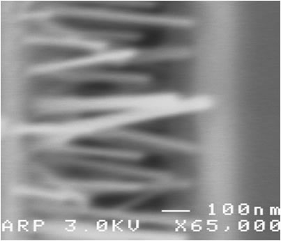
Due to their inherently high surface to volume ratio and diameters of order the Debye length, nanowires (NWs) are natural candidates for high sensitivity chemical and biological sensors. Two of the major challenges facing the use of NWs as sensors are (i) a manufacturable method for large area electrical integration of these quasi one dimensional materials into a CMOS process and (ii) a reliable method for achieving highly specific / selective sensing. The goal of this project is to address these challenges and develop a sensor capable of high sensitivity and selectivity detection of explosives. We have achieved directed growth and integration of ZnO nanobridge devices using photolithographically patterned carbonized photoresist and vapor transport. This carbonized photoresist method avoids the use of metal catalysts, seed layers, and pick and place processes. Growth and electrical connection take place simultaneously for many devices. Three terminal operation and gate enhanced sensitivity to UV light and oxygen has been demonstrated. Work is underway to achieve sensor specificity through functionalization of the surfaces of the nanobridge devices. This project is a collaboration with ARL.
Support provided by: Army Research Laboratory, ONAMI
Dates: August 2008 - December 2011
Investigators: J. Conley (PI) and V. Remcho (co-PI)
Multiple Electron-Hole Pairs for Photovoltaic Devices
A number of recent discoveries make carbon nanotubes (CNTs) a promising material for photovoltaic applications. This project involves using the unique electronic properties of carbon nanotubes to realize multiple electron-hole pair generation, a way to potentially improve the efficiency of photovoltaic devices. Exciton binding energy must be reduced for CNTs to be a useful absorbing material in photovoltaic applications. We study how CNT exciton binding, and related optoelectronic properties, can be optimized by ALD dielectric coatings
Support provided by: Office of Naval Research, ONAMI
Dates: November 2009 - September 2010
Investigators: E. Minot (PI) and J. Conley (co-PI)
Graphene Spin Transistors
The goal of the proposed research is to demonstrate a graphene-based spin field-effect transistor (spinFET). The graphene spinFETS will consist of spin selective, ferromagnetic metal source and drain contacts on a single-layer graphene (SLG) or few-layer graphene (FLG) channel. Spin transport through SLG over micrometer length scales at room temperature has recently been demonstrated in such a system. The spinFETs will additionally have a gate which will affect the conductivity from source to drain by changing the spin orientation of electrons passing through the channel either by Rashba spin-orbit coupling or ferromagnetic exchange coupling. Such devices can potentially be extraordinarily fast because they can operate on the spin of electrons while balistically in transit between the source and drain.
Support provided by: Army Research Laboratory, ONAMI
Dates: July 2008 - July 2010
Investigators: A. Jander (PI), J. Conley (co-PI), R. Solanki (co-PI, PSU)
Nano-Piezoelectric Energy Harvesting
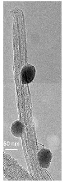
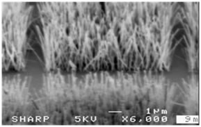
The promise of wireless devices self powered by ambient energy has made "energy harvesting" a hot topic. A 2006 report by Z.L. Wang, et al. demonstrated the possibility of using ZnO nanowires (NWs) to generate piezoelectricity from mechanical vibrations or movements. However, despite the promise of this approach and the extremely high level of interest, nano piezoelectric-based energy harvesting has not been widely investigated. This project involves hydrothermal growth using a microwave oven of piezoelectric ZnO nanowires on a variety of substrates (Kevlar, Si, Pt, etc.), dielectricphoretic alignment of nanowires for device applications, and impedance spectroscopy characterization of ZnO NWs dispersed in solvents.
In addition, new Pb-free piezoelectric materials are investigated for biomedical energy harvesting applications as well as high temperature (T < 400°C) piezoelectric materials for aerospace applications. This project is a collaboration with Pacific Northwest National Lab (PNNL).
Support provided by: Office of Naval Research, ONAMI
Dates: November 2008 - September 2010
Investigators: J. Conley (PI), D. Cann (co-PI), B.J. Gibbons (co-PI), J. Holbery (co-PI, PNNL), and C. Huang (co-PI, PNNL)
General Research Interests:
Dr. Conley's current research interests include atomic layer deposition, metal/insulator/metal devices (MIM & MIIM tunnel diodes, RRAM / memristors, and MIM high-κ capacitors), internal photoemission (IPE), thin film transistors, electron spin resonance (ESR) identification of point defects that play a role in reliability and radiation induced instabilities in novel electronic materials, and directed integration of nanomaterials and devices.
Updated 07/2014