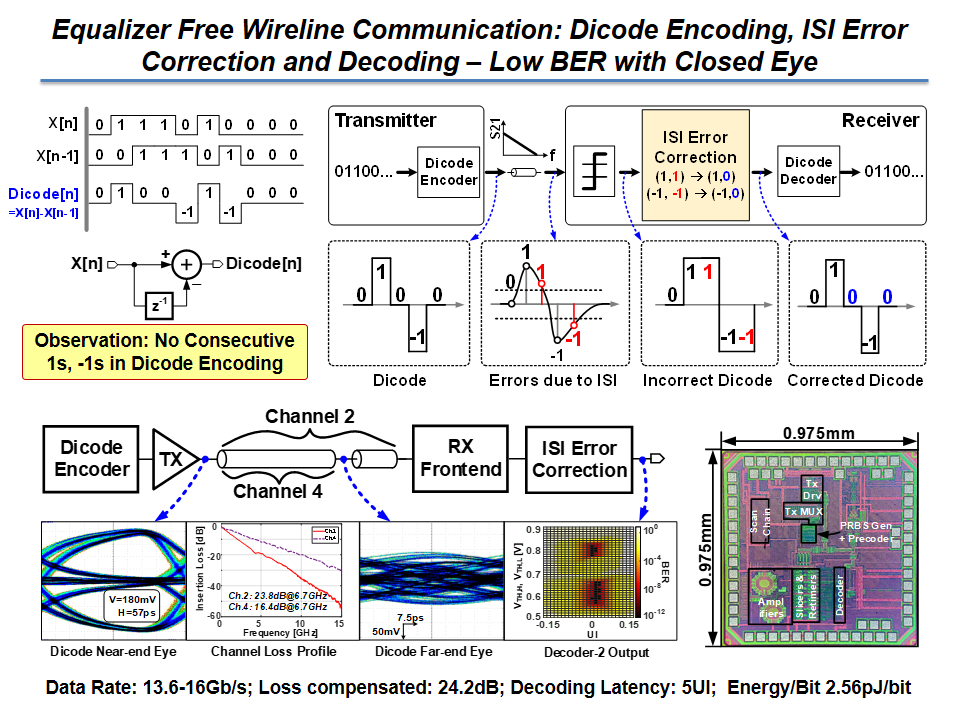
We present an alternative strategy for communicating on bandwidth limited wireline channels without using conventional equalizers (FFE, DFE, CTLE): Dicode
encoding and sequence detection decoding technique for lowbandwidth FR-4 channels. The key observation is that dicode encoded data have no consecutive 1s or -1s. With this known information, the sequence detector at the receiver can correct errors due to inter-symbol interference. Implemented in 65nm CMOS, the proposed highly digital encoding and decoding approach can compensate for up to 24.2dB and 21.4dB loss with 2.56pJ/bit and 2.66pJ/bit efficiency while operating at 13.6Gb/s and 16Gb/s, respectively.
Compared to the state-of-the-art Viterbi-based transceivers, the proposed transceiver achieves 4x better energy efficiency, 3x higher data rate, and 30x lower latency while equalizing 3dB higher channel loss.
[CICC 2019] - Nominated for the Best Student Paper Award
Thrust #2: New Line-Coding Schemes for Channel Equalization - iPWM
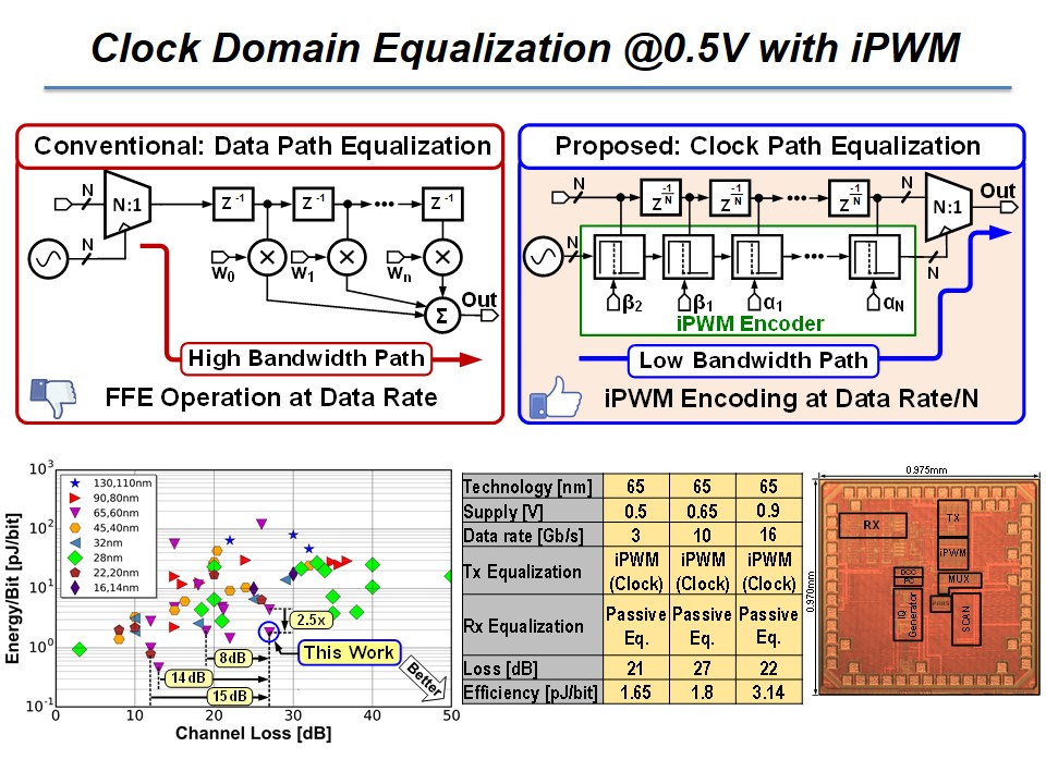
Conventional data equalization is performed by adding a filter on the high-speed data path.
This requires the signal processing to be performed at high bandwidth, which results in higher power consumption and poor energy efficiency and inability to perform equalization at low supply voltages. By leveraging our iPWM encoding, we propose clock domain signal processing transceiver architecture.
In the proposed transceiver, equalization is performed in the subrate clock at very-low speeds, which then encode the data on the final multiplexer.
This helps to equalize heavy channel loss even at 0.5V. The proposed scheme is demonstrated on a 3-to-16Gb/s transceiver operating from 0.5-to-0.9V and equalizing 27dB Loss at 10Gb/s with the energy efficiency of 1.8pJ/bit.
[ISSCC 2018]
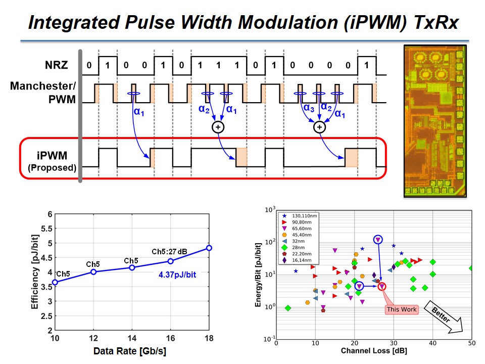
We invented a new encoding/modulation scheme to efficiently equalize lossy wireline channels.
Our encoding scheme - integrated pulse width modulation (iPWM) is an improvement over 68 years old Manchester
(PWM) encoding scheme. The proposed encoding is built on the observation that it is possible to reduce inter-symbol-interference (ISI)
by reducing the pulse width of consecutive identical digits or CIDs such as 1111...0000....
A clear benefit over Manchester encoding/PWM is that with iPWM, narrow pulse widths do not need to be precisely reproduced at the transmitter output.
With iPWM encoding, the output driver can be implemented as an unsegmented source series terminated driver.
This reduces the signaling and switching power of the transmitter, which makes the proposed iPWM and energy efficient equalization scheme.
The proposed encoding scheme is demonstrated on a 10-18Gb/s wireline transceiver using 65nm CMOS.
Operating at 16Gb/s, the complete transceiver achieves an energy efficiency of 4.37pJ/bit and can equalize 27dB channel loss.
[ISSCC 2017][TCAS-1 2019]
Thrust #3: Power Scalable, Rapid-on/off Energy Proportional Links
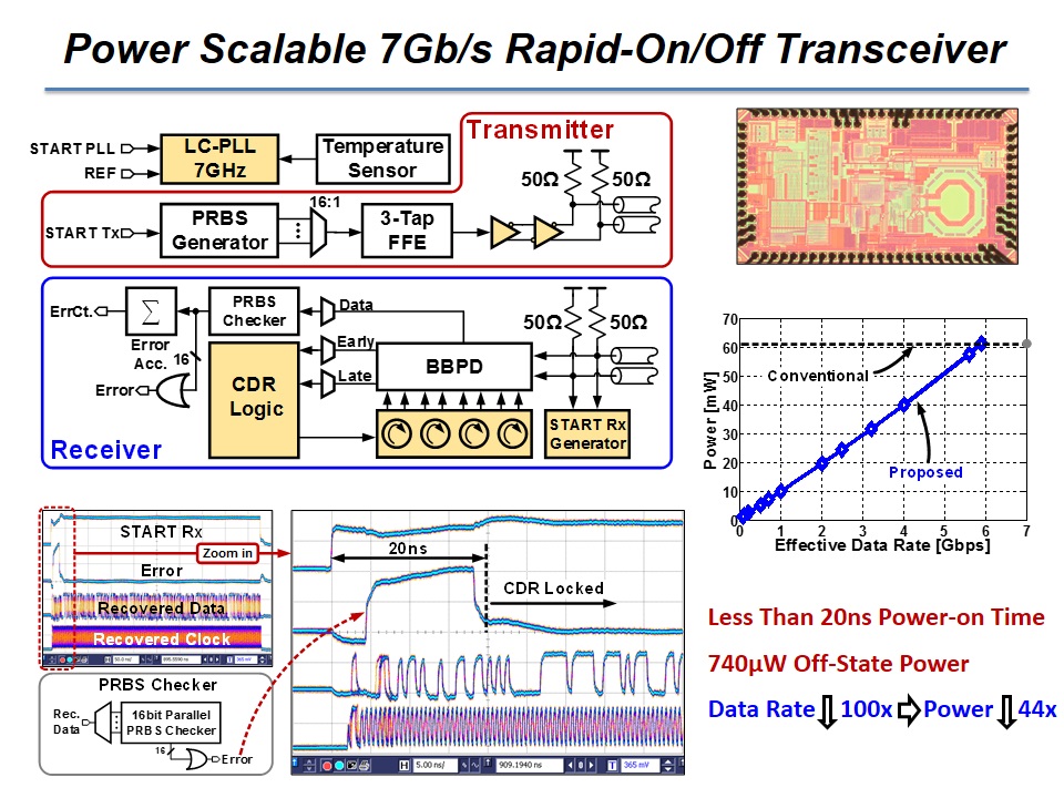
In an energy proportional link, energy consumed by serial link is proportional to the amount of
data communicated. Energy proportionality can be achieved by
scaling the serial link power linearly with the link utilization,
and fine grained rapid power state transition (rapid-on/off) is one
such technique which can achieve this objective. In this research, we developed
architecture and circuit techniques to achieve rapid-on/off in PLL,
transmitter and receiver. The proposed transceiver
demonstrates power scalability with a wide range of link utilization
and, therefore, helps in improving overall system efficiency.
Fabricated in 65 nm CMOS technology, the 7 Gb/s transceiver
achieves power-on-lock in less than 20 ns. Proposed PLL achieves
power-on-lock in 1 ns. The transceiver achieves power scaling by
44 (63.7 mW-to-1.43 mW) and energy efficiency degradation
by only 2.2 (9.1 pJ/bit-to-20.5 pJ/bit), when the effective data
rate (link utilization) changes by 100 (7 Gb/s-to-70 Mb/s). The
proposed transceiver occupies an active die area of 0.39mm2 .
[ISSCC 2015], [JSSC 2015]
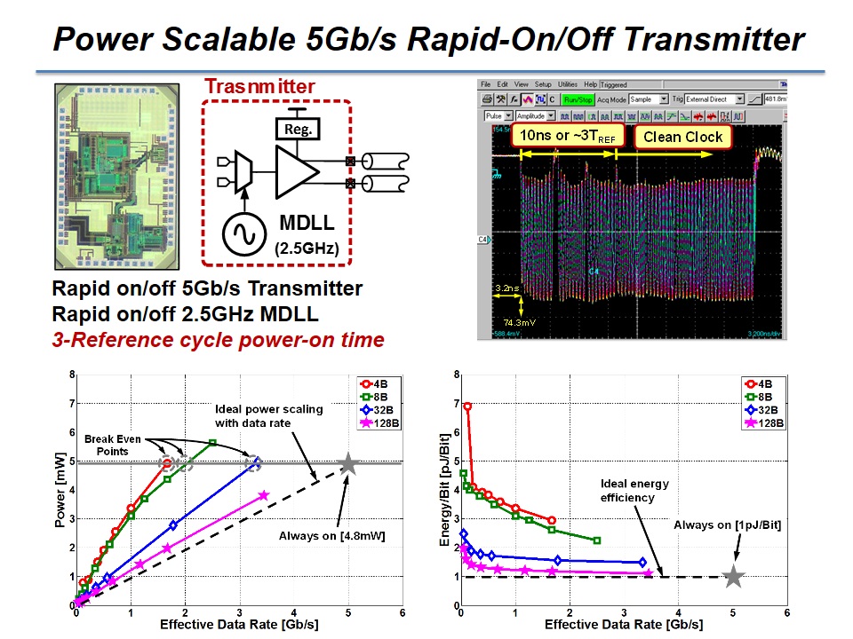
Fabricated in 90nm CMOS technology, the voltage mode driver and the clock multiplier achieve
power-on-time of only 2ns and 10ns, respectively. By using highly scalable digital architecture with
accurate frequency pre-setting and instantaneous phase acquisition, the prototype MDLL-based clock
multiplier achieves 10ns (3 reference cycles) power-on-time, 2psrms long-term absolute jitter at 2.5GHz
output frequency. The proposed fast power-on transmitter architecture consumes 4.8mW/36μW on/offstate
power from 1.1V supply, has 10ns total power-on time, and achieves 100x effective data rate scaling
(5Gb/s-0.048Gb/s), while scaling the power and energy efficiency by only 50x(4.8mW-0.095mW) and
2x(1-2pJ/Bit), respectively. The proposed transmitter occupies an active die area of 0.3mm2.
[ISSCC 2013], [JSSC 2014]
IoT Systems - Harvesters and Sensors
Thrust #1: Source + Switched Capacitor Harvester with No Top and Bottom Plate Switching Loss
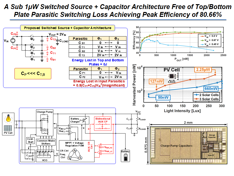
This research presents a 25nW-2.4μW switched-capacitor based energy harvester. The proposed harvester avoids charging and discharging of top and bottom plate parasitic capacitors by switching both the terminals of energy source as opposed to switching just one terminal. As a result, the energy lost in switching the top and bottom plate parasitic capacitors is zero joules, which helps to achieve highly efficient switched capacitor architecture for harvesting sub 1μW energy. The proposed harvester achieves an efficiency of 80% while delivering 1μW output and achieves a peak efficiency of 80.66% at 2.4μW output. It occupies an area of 1.95mm2 in 180nm CMOS.
[CICC 2019]
Thrust #2: VCO Based Temperature Sensor
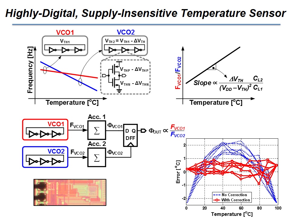
We developed a self-referenced VCO-based temperature sensor with reduced supply sensitivity. The
proposed sensor converts temperature information to frequency and then into digital bits. A novel sensing
technique is proposed in which temperature information is acquired by evaluating the ratio of the output
frequencies of two ring oscillators, designed to have different temperature sensitivities, thus avoiding the
need for an external frequency reference. Reduced supply sensitivity is achieved by employing the voltage
dependence of junction capacitance, thus avoiding the overhead of a voltage regulator.
Fabricated in a 65nm CMOS process, the prototype can operate with supply voltages ranging from 0.85V to 1.1V. It achieves
supply sensitivity of 0.034C/mV and an inaccuracy of ±0.9oC and ±2.3oC from 0-100oC after 2-point
calibration, with and without static non-linearity correction, respectively. The proposed sensor achieves
0.3oC resolution, and a resolution FoM of 0.3nJK2. The prototype occupies a die area of 0.004mm2.
[VLSI 2015], [JSSC 2016]